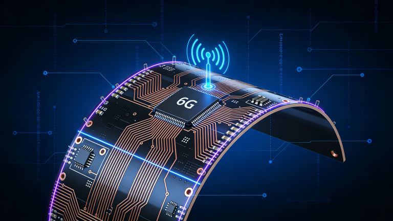
A flexible PCB (FPC) is a thin, bendable printed circuit that can fold, twist, and fit compact 3D spaces. This guide covers structure, materials, stack‑ups, design rules, manufacturing, and real‑world use cases to help global engineers and buyers select the right flex solution.
Introduction
In every new generation of electronic products, there is a clear trend toward devices that are thinner, lighter, and more intelligent, yet packed with far more functionality than before. Flexible printed circuit boards (flex PCBs or FPCs) have become one of the key technologies that make this combination of miniaturization and high performance possible. Instead of relying only on rigid FR‑4 boards and bulky wiring harnesses, designers now route signals through bendable circuits that can fold, twist, and wrap around three‑dimensional structures.
What Is a Flexible PCB?
A flexible PCB (flex circuit or FPC) is a printed circuit board built on bendable polymer film instead of rigid FR‑4. It maintains stable electrical performance while bending, folding, or twisting, making it essential for miniaturized, 3D, and dynamic electronic assemblies.
Unlike traditional rigid PCBs, a flexible PCB reduces weight, shrinks space, removes cables and connectors, and lowers failure points in high‑vibration or compact devices. It is widely used in consumer electronics, medical, automotive, aerospace, and industrial equipment.
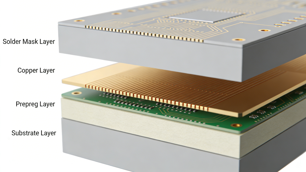
Structure & Types of Flexible PCBs
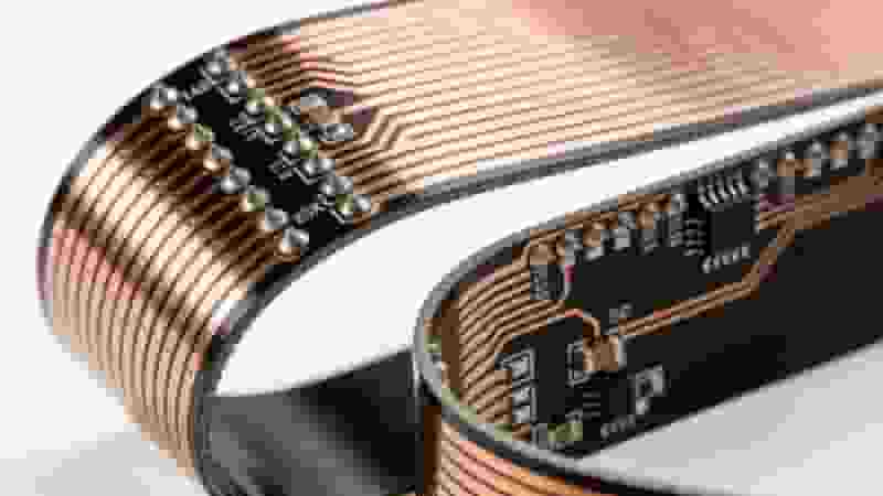
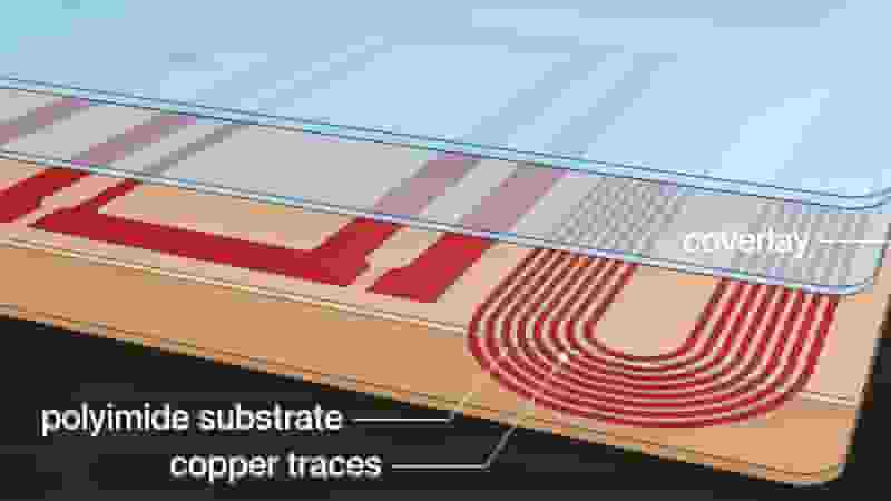
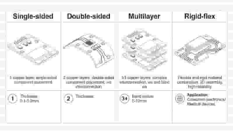
A single‑sided flexible PCB is the simplest form of flex circuit, with copper on only one side of the flexible substrate and a coverlay on top. The structure typically includes a polyimide base film, a single copper layer etched into the required circuit pattern, and a protective coverlay that leaves openings only where pads or fingers are needed for soldering or connection. Because there is only one conductor layer, there are no plated‑through vias within the flex area.
Single‑Sided Flex PCB
One copper layer on polyimide film, lowest cost, high flexibility. Used for simple interconnects.
Double‑Sided Flex PCB
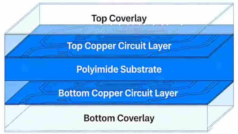
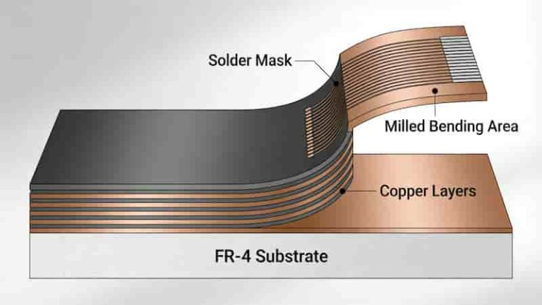
Double‑sided flexible PCBs have copper layers on both sides of the flexible core and use plated‑through holes to connect traces between the two sides. The stack‑up usually consists of a flexible base film, copper on each side, and coverlay applied to both outer surfaces, with drilled and plated vias providing vertical interconnections. This configuration greatly increases routing freedom compared with single‑sided designs while still maintaining good flexibility.
Multilayer Flex PCB
Three+ copper layers with flexible dielectrics. Supports high‑density, controlled impedance, and high‑speed signals.
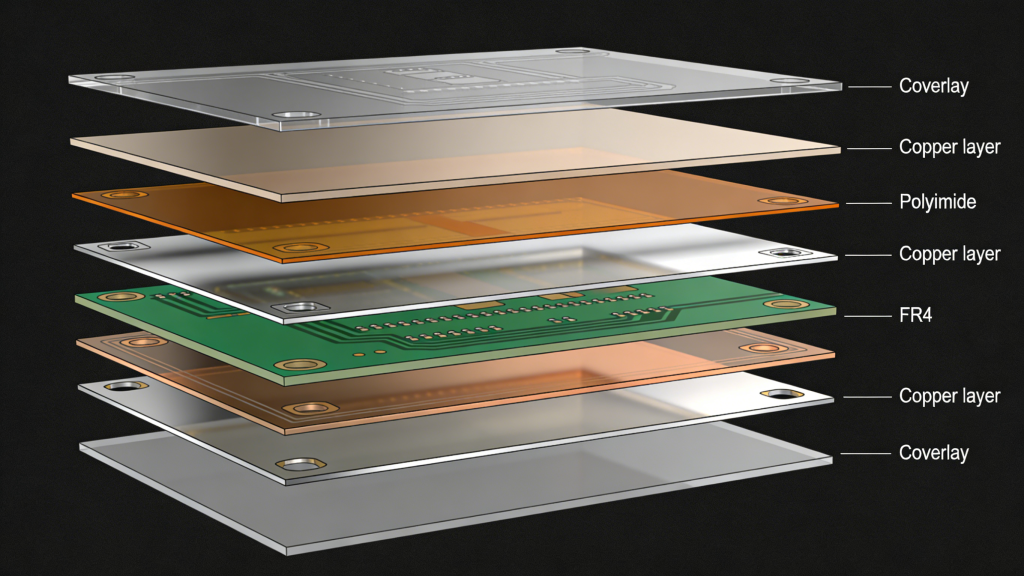
Rigid‑Flex PCB
Combines rigid and flex sections. Ideal for high‑reliability assemblies that need component mounting and bending.
Core Materials for Flexible PCB
Material selection directly defines the reliability, bend life, and cost of a flexible PCB.
Base Substrates
- Polyimide (PI): High temperature resistance, long flex life, used in medical, automotive, aerospace.
- Polyester (PET): Cost‑effective for static flex in consumer products.
Copper Foils
- RA Copper: Ductile, best for dynamic bending and long cycle life.
- ED Copper: Lower cost for static or low‑cycle flex applications.
Protective & Structural Layers
- Coverlay: Replaces solder mask; insulates and protects copper.
- Stiffeners: FR‑4/PI/stainless steel for component mounting areas.
Benefits & Limitations of Flexible PCB
A flexible PCB brings unique advantages but requires proper design.
- Advantages: 3D routing, lighter weight, fewer connectors, higher reliability, miniaturization.
- Limitations: Higher unit cost, sensitive handling, strict bend design rules.
Flexible PCB Design Guidelines
Professional design ensures the flexible PCB meets reliability and performance standards.
- Use minimum bend radius ≥10x total thickness (static) or 20–100x (dynamic).
- Avoid 90° corners; use curved traces in flex zones.
- Keep vias and components out of active bending areas.
- Use symmetric stack‑ups and balanced copper distribution.
- Add stiffeners at connectors and component pads.
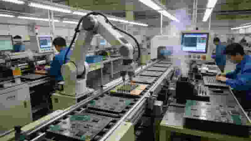
Flexible PCB Manufacturing Process
We produce flexible PCB with precision processes for stable quality:
- Laminate preparation (PI/PET + copper)
- Drilling & via metallization
- Circuit imaging & etching
- Coverlay lamination
- Surface finishing (ENIG, immersion tin, etc.)
- Profile cutting & electrical testing
Key Industrial Applications
The flexible PCB is irreplaceable in these sectors:
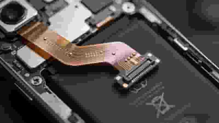
- Consumer Electronics: Smartphones, wearables, cameras, foldable devices
- Medical: Implants, sensors, diagnostic devices, wearable monitors
- Automotive: ADAS, infotainment, lighting, sensors
- Aerospace & Industrial: Avionics, robotics, tight‑space control systems
Flexible PCB vs Rigid PCB
| Feature | Flexible PCB | Rigid PCB |
|---|---|---|
| Bendable | Yes | No |
| Weight & Size | Light, thin, 3D | Bulky, fixed shape |
| Reliability | High (fewer connectors) | Good |
| Cost | Higher | Lower |
Summary
A flexible PCB is a core interconnection solution for modern compact, high‑reliability electronics. With the right materials, design, and manufacturing, it greatly improves product performance while reducing size and failure risks. For global industrial buyers and engineers, selecting a professional flex PCB partner ensures stable quality and on‑time delivery.
Inquiry & Custom Flexible PCB Quote
We provide professional flexible PCB and rigid‑flex PCB manufacturing for global export, supporting prototypes to mass production. Our engineering team offers DFM review, material selection, and customized solutions for medical, automotive, consumer, and industrial projects.
Contact us today for your free quote, design review, and sample support!
Email: chen2351392011@gmail.com
Rigid-Flex PCB Manufacturing & Prototype Services
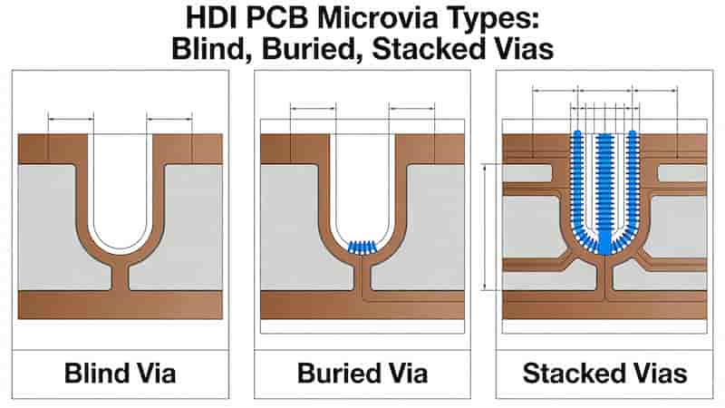
HDI PCB Layout and Basic HDI Design Guidelines
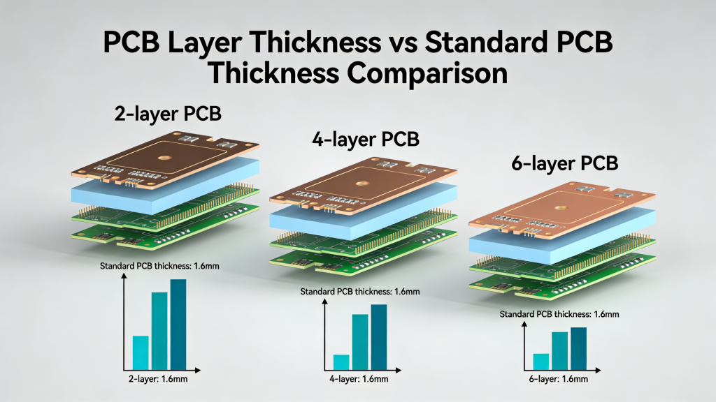
Standard PCB Thickness – The Complete Guide for Engineers & Buyers
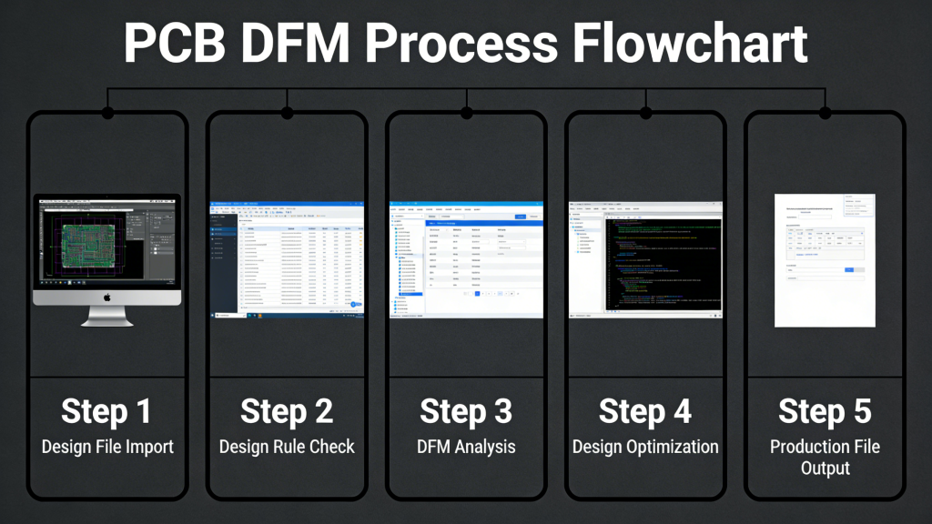
Design for Manufacturability and Assemblability of Printed Circuit Board
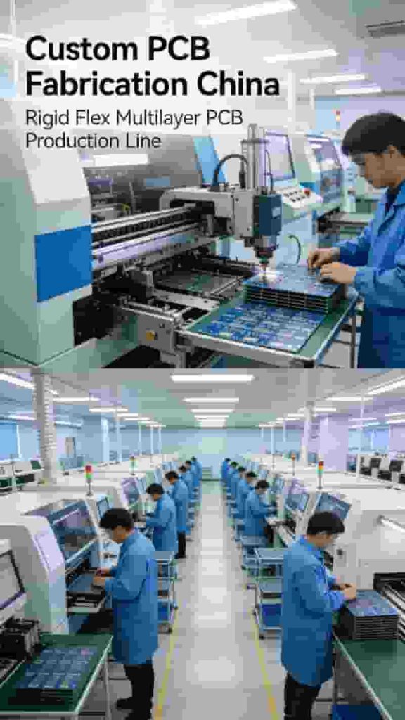
Custom PCB Fabrication in China – Rapid Prototyping & Mass Production