|

Plated Through Holes (PTH) for Printed Circuit Boards: Complete Engineering Guide

Plated Through Hole PTH basic structure PCB copper barrel

Plated Through Holes (PTH) are the foundation of reliable multilayer PCB connectivity. This guide covers PTH design, manufacturing, IPC standards, quality control, and best practices for industrial buyers and engineers.

What Are Plated Through Holes (PTH) in PCBs?

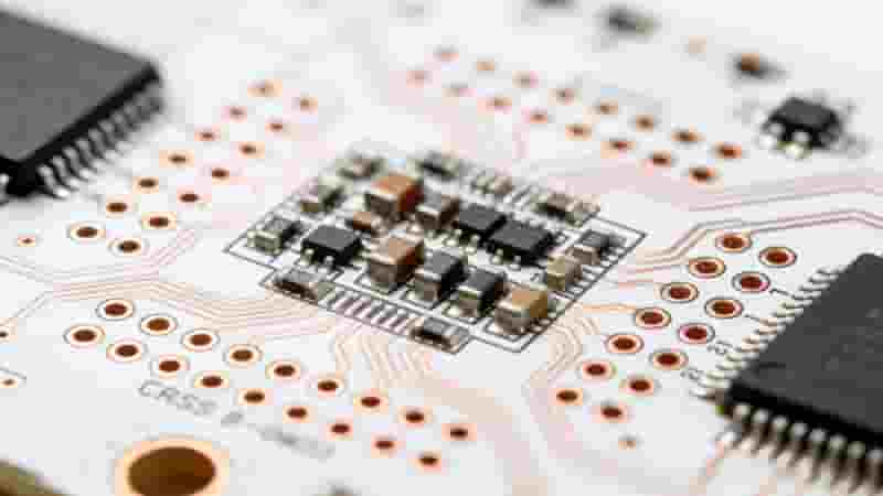
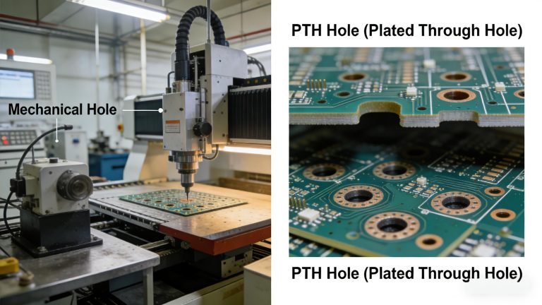
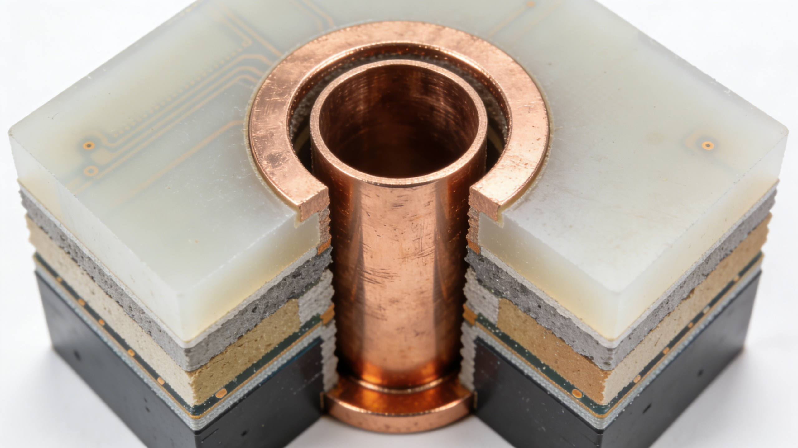
A Plated Through Hole (PTH) is a drilled hole through the PCB substrate with a continuous copper layer plated on the inner wall. It creates stable electrical and mechanical connections between top, bottom, and inner layers of multilayer PCBs.

Plated Through Hole PTH basic structure PCB copper barrel

Unlike non-plated holes, PTH supports component leads, conducts signals and power, and ensures structural stability for high-reliability electronic assembly devices.

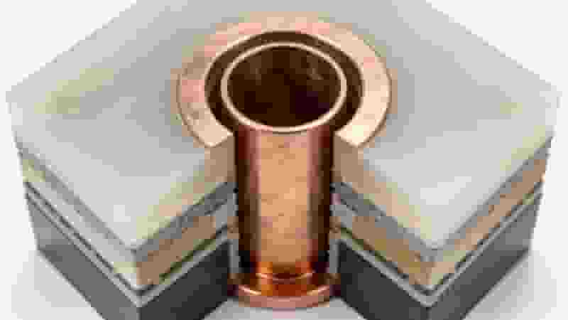
Core Structure of Plated Through Holes

A standard PTH includes these key components:

  • Drilled hole through PCB core and prepreg
  • Electroless copper plating base layer
  • Electrolytic copper barrel for conductivity
  • Annular ring for pad connection
  • Solder mask opening for protection
PTH cross section details annular ring copper barrel PCB

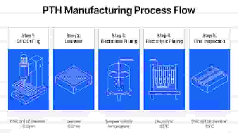
PTH Manufacturing Process (IPC Compliant)

Our PTH production follows strict IPC standards to ensure consistency and reliability:

  1. Drilling: High-precision CNC drilling for clean holes
  2. Desmear: Remove resin residue to improve adhesion去黏膜:去除树脂残留物以提升附着力
  3. Electroless plating: Deposit thin conductive copper layer
  4. Electrolytic plating: Build required copper barrel thickness
  5. Panel plating: Uniform thickness across entire PCB panel
  6. Inspection: Verify plating quality and hole alignment
PTH manufacturing process flow PCB IPC standard

IPC Standards for Plated Through Holes

PTH design and quality are governed by global IPC standards recognized by international buyers:

  • IPC-A-600: Acceptability of printed boards – PTH visual criteria
  • IPC-6012: Qualification and performance for rigid PCBs
  • IPC-2221: Generic PCB design standard for hole size and annular ring
  • IPC-TM-650: Test methods for PTH reliability and adhesion

We produce PTH for Class 1, 2, and 3 PCBs to meet medical, automotive, aerospace, and industrial requirements.

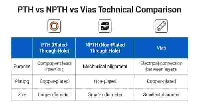
PTH vs NPTH vs Vias: Key Comparison

FeaturePlated Through Holes (PTH)NPTH (Non-Plated)Vias
ConductivityConductiveNon-conductiveConductive
UsageComponent leads, layer connectionMounting, alignment, screwsHigh-density signal routing
SizeLarger diameterVariableSmall, micro-vias
PCB TypeSingle-sided to multilayerAll PCB typesMultilayer & HDI PCBs

PTH Design Rules for Reliable PCBs

Follow these rules to optimize PTH performance and yield:

  • Hole diameter: Match component lead diameter + clearance
  • Annular ring: Minimum 0.05mm per side (IPC Class 2)
  • Aspect ratio: ≤10:1 for standard PCBs
  • Copper barrel thickness: ≥20μm for industrial applications
  • Avoid placing PTH near board edge or high-speed traces
PTH design parameters annular ring aspect ratio PCB

Industrial Applications of Plated Through Holes

PTH technology supports critical electronics across industries:

  • Automotive electronics: Engine control, safety systems
  • Medical devices: Patient monitoring, diagnostic equipment
  • Industrial control: PLC, power supply, automation
  • Telecommunications: Routers, servers, base stations
  • Aerospace & military: High-reliability mission-critical systems

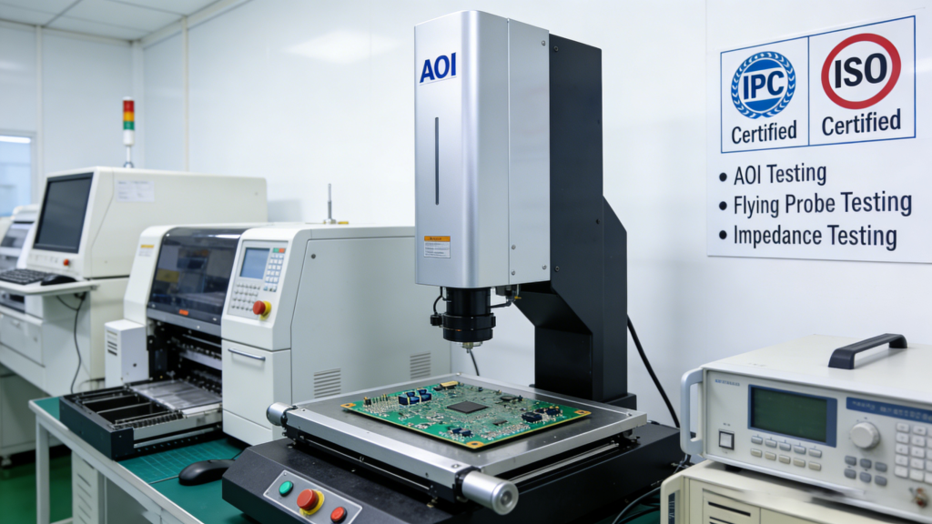
PTH Quality Control & Reliability Testing

Every batch of PTH-enabled PCBs undergoes rigorous testing:

  • Cross-section analysis for copper barrel integrity
  • Thermal stress testing (thermal shock)
  • Solderability testing per IPC standards
  • Electrical continuity and isolation test
  • Automatic optical inspection (AOI)

Summary

Plated Through Holes (PTH) are essential for robust, long-lasting PCB performance. By following IPC standards, precise design, and strict PCB manufacturing control, we deliver PTH PCBs that meet global industrial requirements.

Our PTH capability supports multilayer PCBs from 2-layer to 30+ layers, with tight tolerances and high reliability for export markets.

Need Reliable PTH PCB Manufacturing?

Request a free quote, custom design review, or sample board for your PTH PCB project. We support global export with full technical support and IPC compliance.

Request Quote
Contact Engineering

Single-Sided Flex PCB Bending Radius Static vs Dynamic IPC Standard

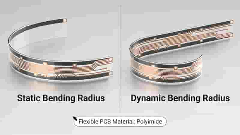
Single-Sided Flexible PCB Design Guide: Bending Radius, Trace Routing and Stiffeners

Posted on
0 Comments
Single-sided flexible PCBs look simple, but poor design on bending radius, trace layout or stiffener placement can quickly lead to cracks and failures. This engineering guide provides practical rules for minimum bend radius, trace routing in flex zones, and stiffener usage to keep single-sided flexible PCB reliable in static and dynamic applications. Introduction to Single-Sided…
Flexible PCB fabrication process flow chart

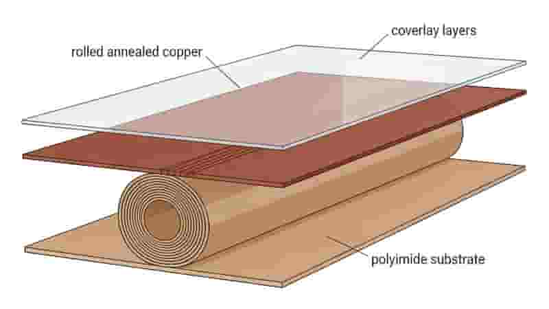
Flexible PCB Manufacturing and Assembly: The Complete 2025 Guide

Posted on
0 Comments
This professional guide covers flexible PCB materials, fabrication, SMT assembly, quality control, and best practices for engineers, buyers, and global importers. Learn how to ensure reliability, consistency, and cost efficiency for your flex PCB projects. Why Choose Flexible PCBs? Flexible PCB devices offer distinct advantages over rigid PCBs, making them ideal for modern electronics with…
PCB Quality Testing AOI Flying Probe Impedance Test IPC ISO Certified

Worry-Free Custom PCB Manufacturing for American Customers

Posted on
0 Comments
Custom PCB solutions built for US industrial buyers, engineers, and procurement teams—ISO & IPC certified, reliable quality, on-time delivery, and full technical support for prototypes to mass production. Our Custom PCB Manufacturing Capabilities We deliver end-to-end custom PCB manufacturing supporting rigid, flex, rigid-flex, HDI, metal-core, and high-frequency boards. Our production lines handle 1–32 layers, precise…
Rigid-Flex PCB Stackup Overview Layer Structure Diagram

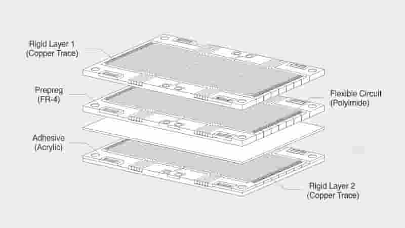
Rigid-Flex PCB Stackup: Professional Design & Manufacturing Guide 

Posted on
0 Comments
Rigid-Flex PCB Stackup is the core of high-performance rigid-flex circuit boards, directly determining reliability, flexibility, signal integrity and service life. This guide covers layer structure, material selection, impedance control, DFM rules, common stackup examples and manufacturing standards for engineers and procurement teams. What Is Rigid-Flex PCB Stackup Rigid-Flex PCB Stackup defines the layered arrangement of…
Single-Sided Flexible PCB SMT Assembly Line

Single-Sided Flexible PCB Fabrication & Assembly Services

Posted on
0 Comments
We provide reliable single-sided flexible PCB manufacturing and full assembly for industrial, medical, automotive, and consumer electronics globally. Jump to: Overview | Capabilities | Process | Comparison | FAQ Single-Sided Flexible PCB Overview A single-sided flexible PCB is a lightweight, bendable circuit with conductive traces on one dielectric layer. It is widely used in compact…
China PCB Prototype Manufacturing Facility

Global PCB Prototype Manufacturers: Top Picks & Why We Excel

Posted on
0 Comments
Discover leading PCB prototype manufacturer options across China, USA, and UK. We deliver 24-hour rapid prototyping, free DFM analysis, and high-reliability PCBs for automotive, medical, aerospace, and industrial applications. Choosing the right PCB prototype manufacturer is critical for validating design functionality, ensuring manufacturability, and accelerating time-to-market. This guide compares leading global suppliers and explains why…

FAQs About PCB PTH Design, IPC Standard & QC Specification

A: Full penetrating drilled hole, electroless base copper, electrolytic thickened copper barrel, outer annular pad and reserved solder mask opening area.

A: IPC-A-600 for appearance acceptance; IPC-6012 for board qualification; IPC-2221 for layout design; IPC-TM-650 for reliability test method.

A: Min annular ring ≥0.05mm per side, aspect ratio controlled ≤10:1, hole wall copper thickness ≥20μm for industrial grade PCB.

A: PTH for component welding + interlayer conduction; NPTH only mechanical fixing without conduction; small-size via dedicated to high-density signal routing.

A: CNC precision drilling → desmear resin removal → electroless copper → electrolytic panel plating → finished dimensional & appearance inspection.

A: Cross-section barrel check, thermal shock cycling test, solderability verification, electrical continuity test and AOI automatic optical scanning.

A: Automotive ECU, medical monitoring equipment, industrial PLC controller, communication server board and aerospace high-reliability modules.

A: NPTH cancels plating process, cuts manufacturing cost while satisfying pure mechanical fixing and assembly positioning requirement.

Similar Posts