Flexible PCB Coverlay: What It Is & How It Works

Flexible PCB Coverlay Lamination Process

Flexible PCB coverlay is a protective polyimide film that protects FPC copper circuits while keeping full flexibility. Learn materials, thickness, comparison with solder mask, manufacturing, and selection for industrial and medical applications.

What Is Flexible PCB Coverlay?

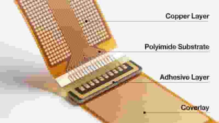
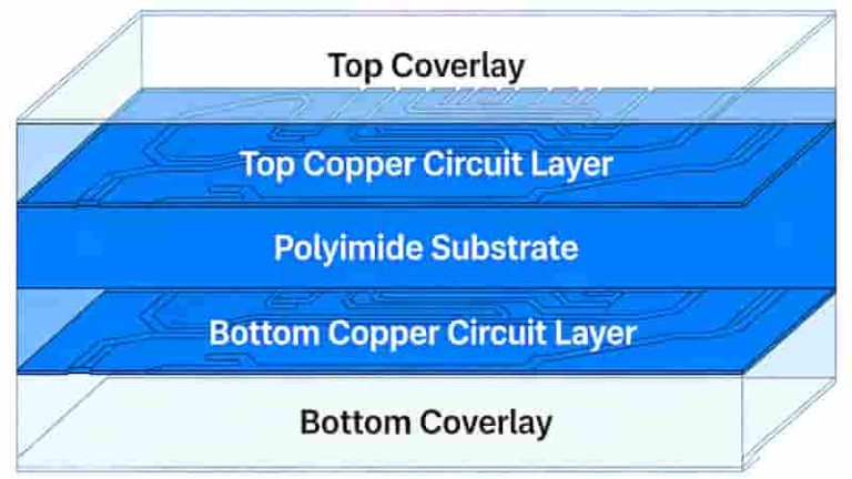
A flexible PCB coverlay, also known as FPC cover layer, is a key protective part for flexible printed circuits. It is made of polyimide film and flexible adhesive, which insulates and protects copper traces from moisture, dust, chemicals and mechanical stress while keeping the FPC bendable and foldable.

Different from rigid PCB solder masks, flexible PCB coverlay is designed for dynamic bending use, making it necessary for wearables, automotive electronics, medical devices and consumer electronics.
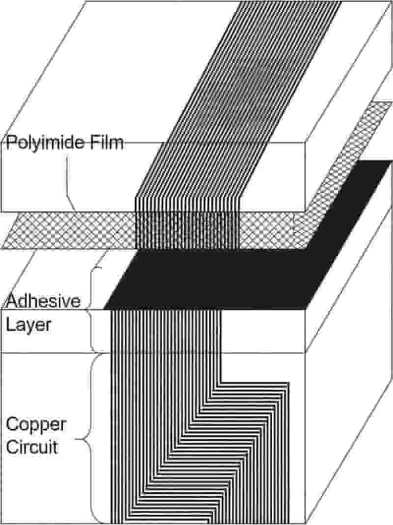
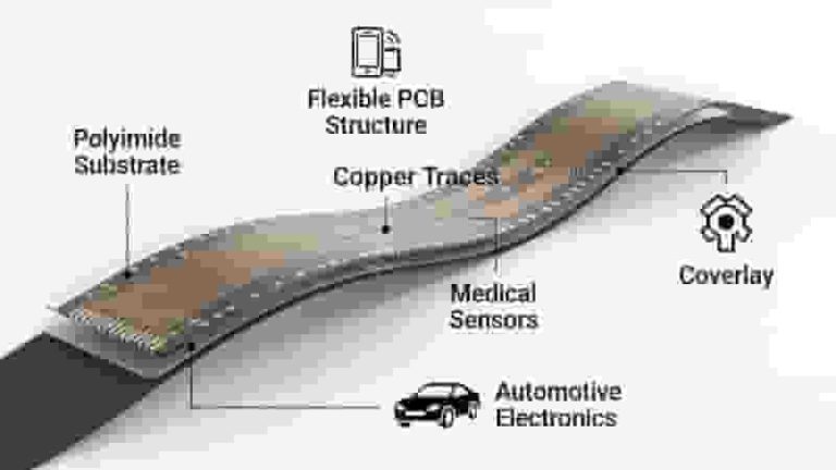
Flexible PCB Coverlay Structure Polyimide Adhesive Layers

Key Functions of Flexible PCB Coverlay

  • Protects copper circuits from corrosion, abrasion and environmental damage
  • Provides high dielectric strength at about 3kV per mil thickness
  • Keeps full flexibility for repeated bending and folding
  • Improves FPC reliability and service life in harsh environments
  • Meets industrial standards for medical, automotive and aerospace use

Flexible PCB Coverlay Thickness Options

Flexible PCB coverlay thickness directly affects flexibility, durability and performance. Standard combinations include polyimide film and adhesive layers:

Polyimide ThicknessAdhesive ThicknessTotal ThicknessBest Application
0.5 mil0.5 mil1.0 milUltra-flexible wearables
1.0 mil1.0 mil2.0 milStandard consumer electronics
2.0 mil1.0 mil3.0 milRugged automotive & industrial

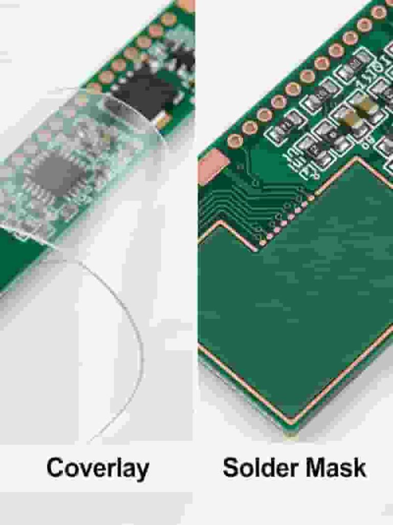
Coverlay vs Solder Mask: Key Differences

Both protect circuits, but flexible PCB coverlay and solder mask serve different design goals:

FeatureFlexible PCB CoverlaySolder Mask
MaterialPolyimide + adhesiveLiquid epoxy polymer
FlexibilityHigh supports dynamic bendingLimited for rigid PCBs
Minimum Dam Size10 mils4 mils
Best ForFPC & rigid-flex boardsRigid PCBs & fine-pitch parts
Flexible PCB Coverlay vs Solder Mask Comparison

Flexible PCB Coverlay Manufacturing Process

  1. Material Selection: High-temperature polyimide film and acrylic or epoxy adhesive
  2. Precision Cutting: Laser or die-cut openings for pads, vias and components
  3. Alignment: Accurate placement on FPC with fiducial markers
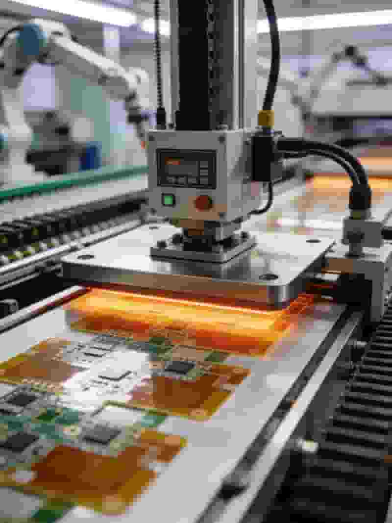
  4. Lamination: Heat and pressure bonding for bubble-free adhesion
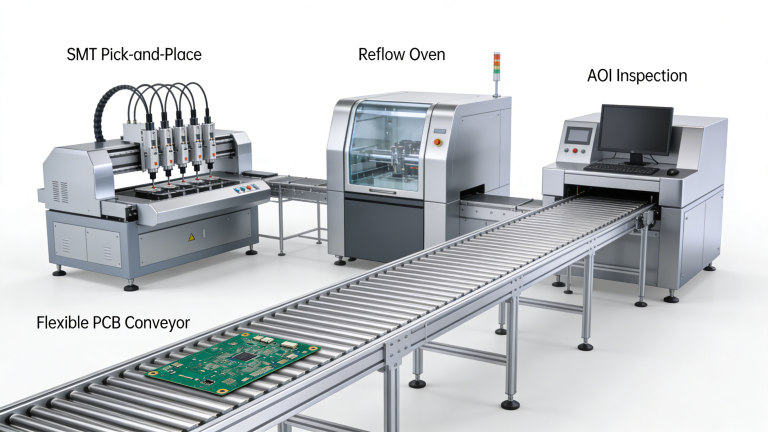
  5. Curing & Inspection: AOI check, flexibility test and dielectric validation
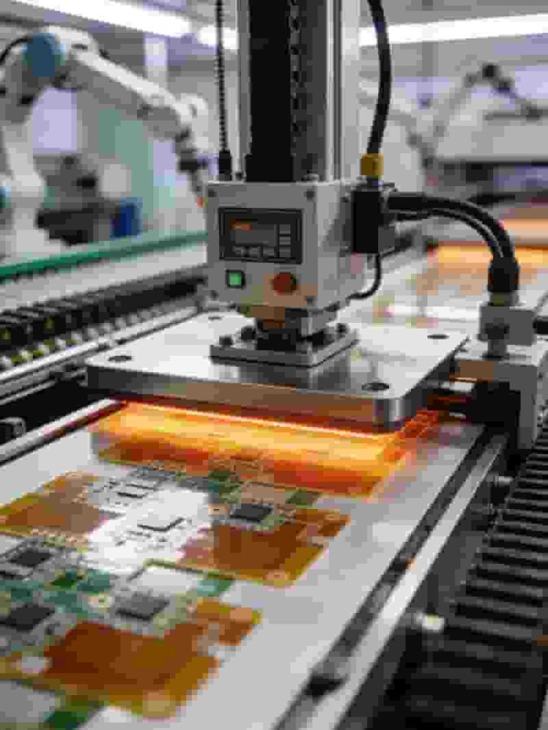
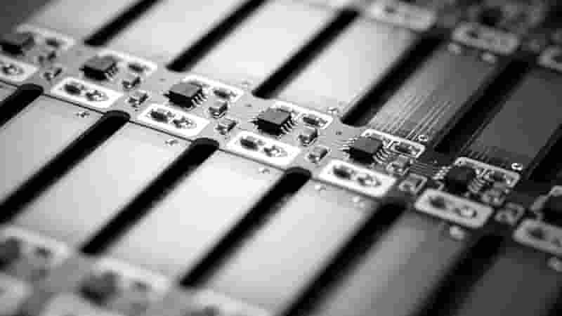
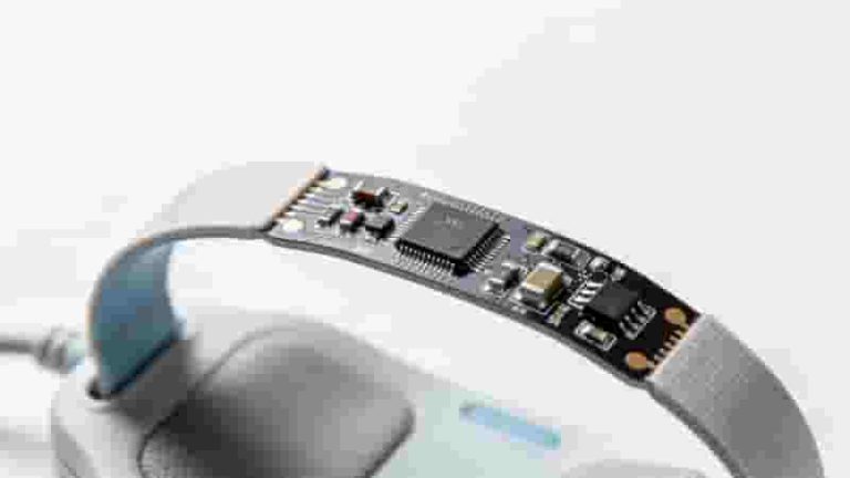
Flexible PCB Coverlay Lamination Process

Industry Applications of Flexible PCB Coverlay

Flexible PCB coverlay supports reliable performance in high-demand industries:

  • Consumer Electronics: Foldable phones, wearables, wireless earbuds
  • Medical Devices: Implantable sensors, wearable monitors, diagnostic tools
  • Automotive: Sensors, lighting, dashboard circuits, infotainment systems
  • Aerospace & Defense: Satellite circuits, avionics, drone controls
  • Industrial & 5G: Robotics, high-speed antennas, flexible solar panels
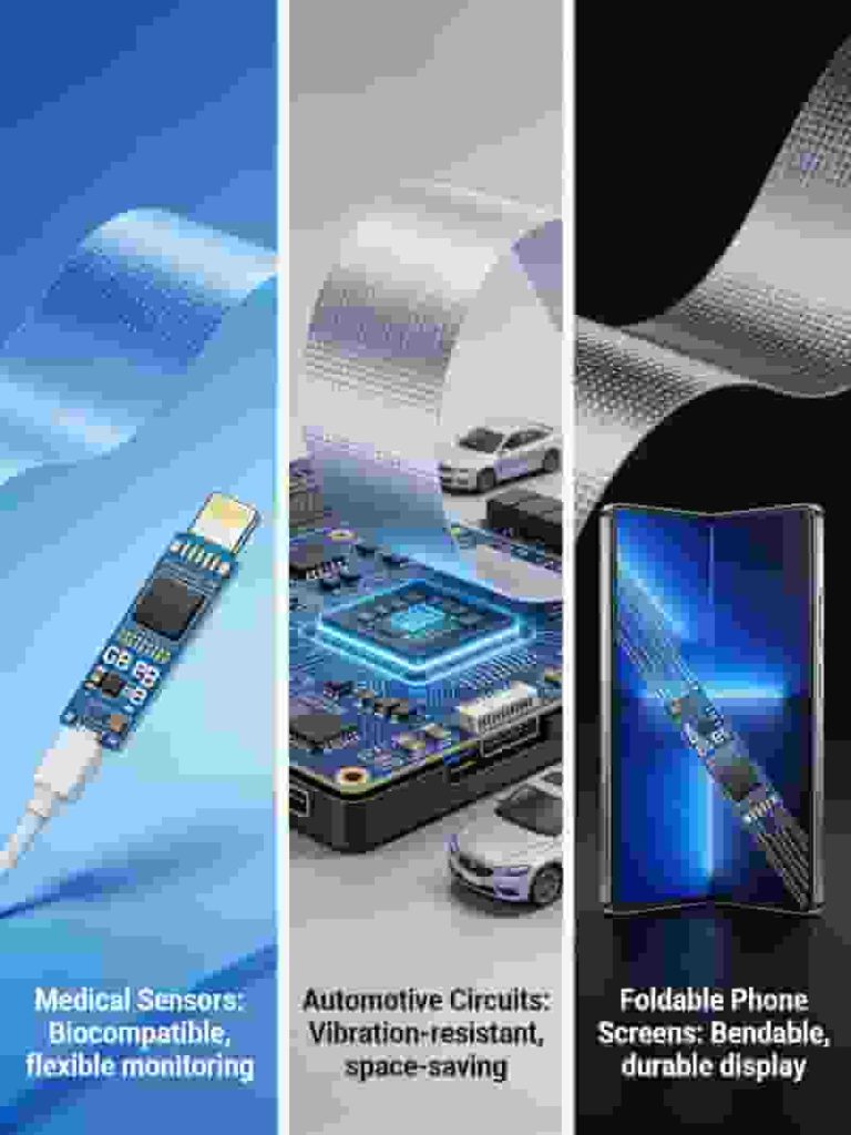
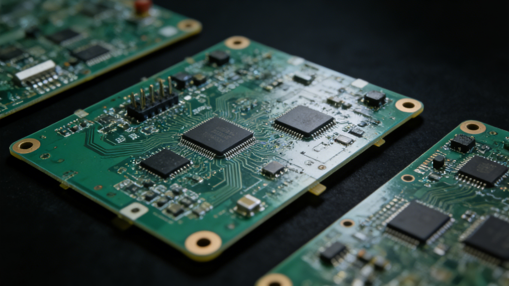
Flexible PCB Coverlay Applications in Medical Automotive Electronics

How to Select the Right Flexible PCB Coverlay

Choose coverlay based on these important factors:

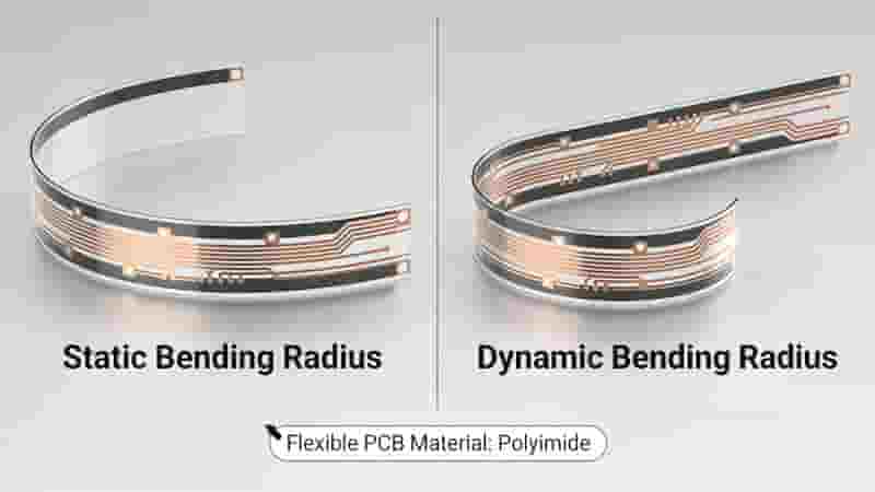
  • Bending radius requirement: thinner film for tighter bending
  • Environment exposure: thicker layers for harsh conditions
  • Dielectric strength needs for high-voltage circuits
  • Copper weight and circuit density
  • Industry compliance for medical, automotive and aerospace

Conclusion

Flexible PCB coverlay is an essential component for reliable and long-lasting flexible circuits. It balances protection, insulation and flexibility to meet modern electronic needs. Choosing the right material and thickness ensures the best performance for your FPC design.

Need Professional Flexible PCB Support?

Get FPC design, material selection and manufacturing support for your global export projects.

Request Free Quote & DFM Check
Multilayer PCB stackup basics core prepreg copper layers structure

Multilayer PCB Layer Stackup And Thickness Guide: Standard 4‑Layer to 14‑Layer Configurations

Posted on
0 Comments
Multilayer PCB stackup and thickness directly determine signal integrity, EMC performance, mechanical stability and manufacturability. This professional guide covers core principles, key parameters, standard stackups from 4‑layer to 14‑layer, thickness selection and engineering best practices for industrial electronics, high‑speed designs and critical applications. Why Multilayer PCB Stackup And Thickness Matter Modern electronics demand smaller size,…
Step-by-step PCB via manufacturing: drilling, plating, filling and capping

PCB Vias: Complete Guide to Types, Design, Reliability and Performance

Posted on
0 Comments
A full professional overview of PCB vias including definitions, functions, types, manufacturing, reliability factors and advanced technologies for high‑performance multilayer printed circuit boards. Introduction: Definition, Role, and Types of Vias in PCBs A via is a vertical electrical connection between layers in a printed circuit board. Vias enable traces to transition between layers to facilitate…
Metal Core PCB Structure Diagram MCPCB Layer Composition

Professional Metal Core PCB (MCPCB) Manufacturing & Custom Service in China

Posted on
0 Comments
We specialize in high-quality Metal Core PCB (MCPCB) design, prototyping, and mass production. Our advanced manufacturing capabilities deliver superior thermal management solutions for LED lighting, automotive, power electronics, and industrial applications, with strict compliance to international standards. What is Metal Core PCB (MCPCB) Metal Core PCB (MCPCB), also known as Insulated Metal Substrate (IMS) or…
PCB Lead Time Comparison Prototype and Mass Production Volume

Key Differences Between Prototype and Production PCBs Explained

Posted on
0 Comments
Understanding prototype PCBs and production PCBs is essential for engineers, buyers, and project managers. This guide breaks down critical differences in lead time, cost, design flexibility, materials, testing, quality standards, and manufacturing processes to help you make informed decisions for your electronics projects. Introduction Printed circuit boards are foundational to nearly all electronic devices. The…
Flexible LED PCB bendable circuit board

Professional LED PCB Manufacturing & Assembly Services

Posted on
0 Comments
We provide professional LED PCB manufacturing and assembly services with superior heat dissipation. ISO 9001 certified, fast turnaround and competitive pricing for global lighting, automotive, medical and industrial clients. Get Instant QuoteView Capabilities Manufacturer – Your Trusted Partner for LED Circuit Board Manufacturing We focus on high-quality LED PCB manufacturing and assembly, delivering full solutions…
PCB DFM analysis engineering support service

How to Choose the Right PCB Manufacturer and Supplier: Full Professional Guide

Posted on
0 Comments
When starting a new electronics project, selecting a reliable PCB manufacturer is critical to success. This guide helps engineers and procurement teams evaluate quality, certifications, lead time, testing, cost, and communication to pick the best supplier for prototypes and mass production. Why Choosing the Right PCB Manufacturer Matters In the fast‑paced electronics industry, the Printed…

FAQs About Flexible PCB Coverlay

A: It is a polyimide protective film for FPC. It insulates copper traces against moisture, abrasion and corrosion while retaining excellent bendability.

A: Total thickness options are 1.0 mil, 2.0 mil and 3.0 mil. Thinner types suit wearables, while thicker ones fit industrial and automotive products.

A: Coverlay is flexible polyimide film for FPC; solder mask is rigid epoxy coating for regular PCBs. Coverlay supports repeated bending, while solder mask has smaller minimum dam size.

A: Material selection → precision cutting → alignment → thermal lamination → curing and full performance inspection.

A: It is commonly applied in consumer electronics, medical devices, automotive, aerospace, industrial automation and 5G equipment.

A: Consider bending radius, working environment, dielectric requirements, circuit density and relevant industry compliance standards.

Similar Posts