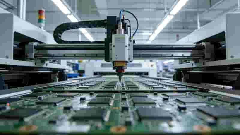
Discover industry-leading performance with our nano-coated PCB stencils. Engineered to support high-precision SMT printing processes, professional nano surface treatment greatly improves stencil durability, stabilizes solder paste deposition quality, and cuts routine maintenance workload, helping your entire PCB assembly line run stably and efficiently.
Why Choose Nano-Coated PCB Stencils For SMT Production
Nano-coated SMT stencils deliver stable high-precision printing while extending service life and lowering overall production costs. We fully understand strict standards of modern surface mount assembly, and tiny performance improvements on stencils will directly reduce solder defects and raise your finished PCB qualification rate.
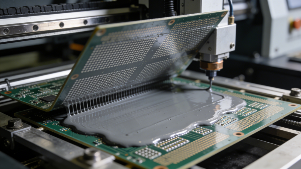
Our professional nano coating forms ultra-smooth superhydrophobic non-stick surface, effectively reducing solder paste residue on aperture walls and stencil bottom. Every printing pattern remains clear and accurate, bringing less production downtime, consistent batch quality and easier daily cleaning work.
No matter you process high-density multilayer PCBs or ultra-fine pitch circuit designs, our customized nano stencils provide reliable mechanical stability and printing precision to match all sophisticated SMT assembly requirements.
Key Benefits Of Nano Coating SMT Stencils
Upgrading to nano-treated PCB stencils upgrades your whole SMT workflow in precision, stability and long-term cost performance:
- Higher Printing Accuracy: Low surface energy nano layer ensures accurate solder paste transfer, avoids smudging and deviation, perfectly adapts fine-pitch BGA & QFN PCB components
- Less Maintenance & Shorter Downtime: Minimal solder paste adhesion greatly cuts frequent stencil cleaning cycles, improves continuous production capacity
- Enhanced Wear Resistance & Long Lifespan: Nano protective layer reduces surface abrasion and corrosion, extends usable cycles and decreases frequent stencil replacement expenses
- Stable Paste Release Performance: Consistent solder deposit shape reduces bridging, voids and poor soldering defects on assembled PCB boards
Suitable Industries & Complex PCB Applications
Our custom nano SMT stencils serve global high-standard electronics manufacturing scenarios with strict precision and reliability requirements:
| Industry Field | PCB Application Features | Nano Stencil Advantages |
|---|---|---|
| Consumer Electronics | Miniature HD PCB, dense component layout | Clear fine pattern printing |
| Automotive Electronics | High volume, vibration resistant PCB assembly | Stable long-term printing consistency |
| Medical Device PCBs | Ultra-high precision, zero tolerance error | Reliable medical-grade solder quality |
| Telecommunication Hardware | High frequency complex circuit PCB designs | Stable ultra-fine aperture performance |
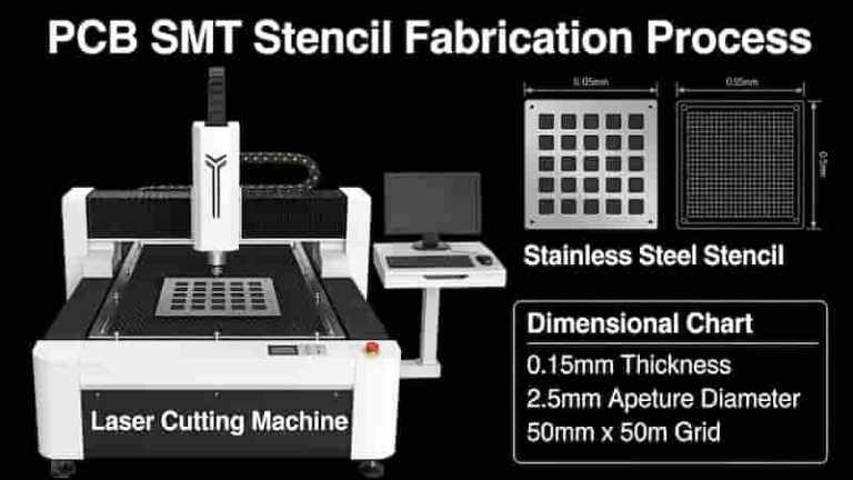
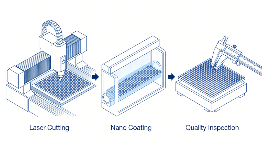
Full Manufacturing Process Of Nano-Coated Stencils
High-quality nano layer PCB stencils require standardized precision procedures at every production stage:
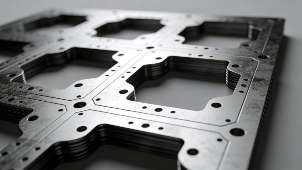
- Premium Material Selection: Adopt high-grade stainless steel foil with stable rigidity and dimensional accuracy, adapt high-volume long-time SMT printing work
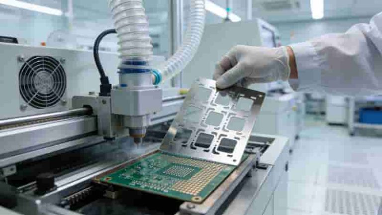
- High Precision Laser Cutting: Advanced laser etching forms accurate uniform apertures, matching ultra-fine pitch PCB layout requirements perfectly
- Professional Nano Coating Application: Uniform ultra-thin nano film covers stencil surface and hole walls, forms anti-adhesion self-cleaning performance
- Post-treatment & Shape Calibration: Stabilize coating structure, ensure no size deformation and stable matching with SMT printers
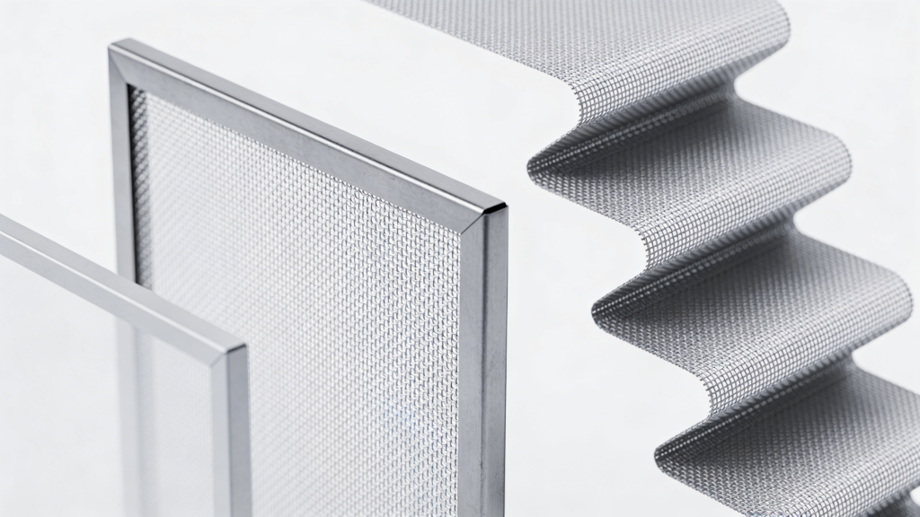
Different Types Of Custom Nano SMT Stencils
We provide diversified nano-coated steel stencils customized according to your PCB prototype, mass production and assembly technology:
- Framed & Frameless Nano Stencils: Frameless stencils suit fast prototype switching; framed stencils ensure high alignment stability for large-batch PCB production
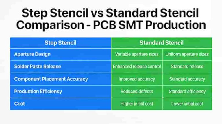
- Step Nano Stencils: Multi-thickness design fits mixed-height components, realizes accurate solder paste thickness control for complicated PCB assembly
- Electroformed Nano Stencils: Ultra-smooth aperture wall, extreme precision for microelectronics and ultra-fine pitch PCB circuit printing
Strict Quality Assurance & Precision Inspection
Reliable SMT nano stencil quality is the foundation of stable PCB finished product yield. Every product undergoes full-process quality control before delivery.
We adopt high-resolution dimensional detection equipment to verify aperture tolerance, coating uniformity, surface smoothness and flatness. All parameters fully comply with international SMT industry specifications, support strict quality audit requirements from global electronics buyers.
Full inspection covers coating durability, printing consistency and anti-paste residue performance, guarantee long-time stable operation of your nano-coated PCB stencils on automated production lines.
Request Your Custom Nano Stencil Quote
Start your high-precision PCB SMT project with professional nano-coated PCB stencil solutions. We support DFM optimization, full parameter customization, fast quotation and reliable global delivery service.
Please send your stencil type, size, thickness, fiducial requirements, electropolishing needs and special process specifications. We will reply your detailed professional quotation within 2–8 hours and assist you optimize stencil design for better PCB assembly yield.
Get Free Custom Nano Stencil Quote Now
Full Name
Email Address
Stencil Type
Stencil Size (mm)
Stencil Thickness & Side Requirements
Fiducial Mark & Electropolishing Requirements
Special Custom Process & Design Files (ZIP/RAR only, Max 20MB)
Related Reading: Step Stencil Guide | SMT Stencil Cleaning Methods | Laser Cut vs Etching PCB Stencils
We provide DFM verified PCB & stencil products with fast production speed and 100% stable quality guarantee worldwide.
PCB Manufacturing Process Part 1: MI, Cutting & Drilling – Complete Industrial Guide
Gold Finger PCB Fabrication & Manufacturing Service
What Are Aluminum PCBs Used For? Applications and Benefits for Industrial Buyers
Multilayer Flexible PCB Manufacturer | Custom 4–16 Layer Flex Circuits
Flexible PCB: Complete Materials, Design & Industrial Application Guide