|

Flying Probe Testing for PCB: The Complete Professional Guide

Advantages of Flying Probe Testing for PCB

Flying Probe Testing for PCB is a fixtureless electrical testing method widely used for prototype, low-volume and high-mix printed circuit board production. It accurately detects opens, shorts, wrong components, reverse polarity and soldering defects without expensive custom fixtures, making it the top choice for engineering verification and small-batch manufacturing.

What is Flying Probe Testing?

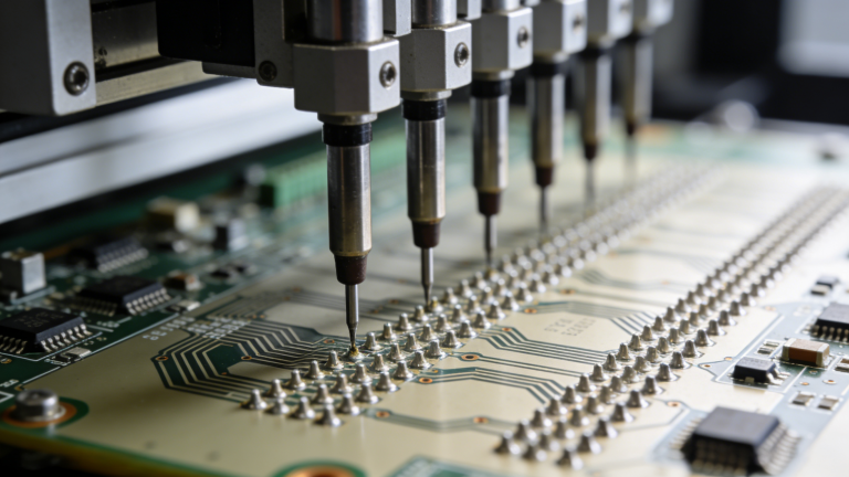
Flying Probe Testing for PCB is an automated electrical test method that uses movable probes to contact test points one by one to verify circuit integrity and component functionality. Unlike traditional bed-of-nails testers, it requires no custom fixture, which greatly reduces upfront cost and lead time.

Modern flying probe systems support both bare PCB and assembled PCBA testing, covering electrical opens, shorts, wrong components, reversed polarity, missing parts and poor solder joints.
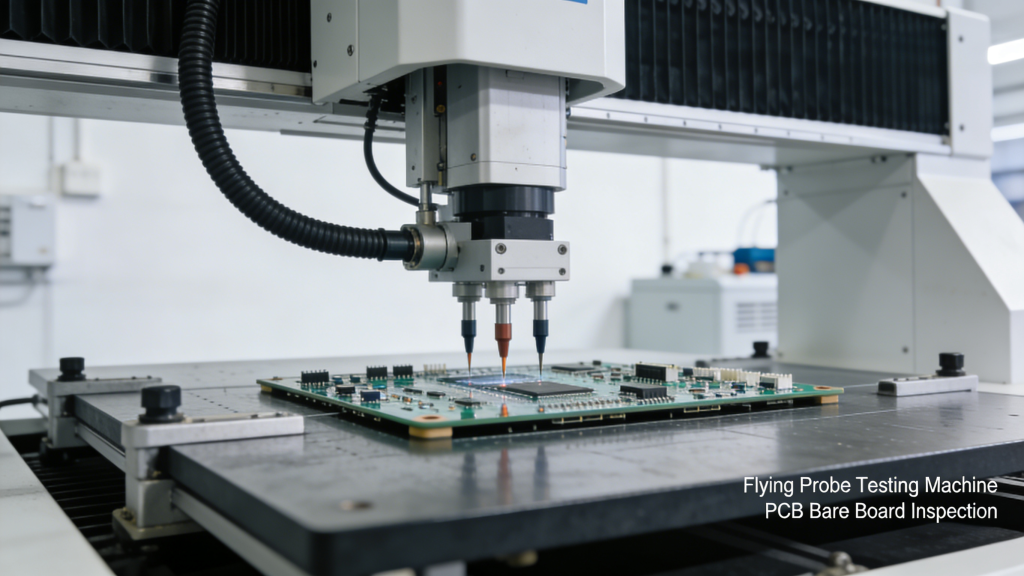
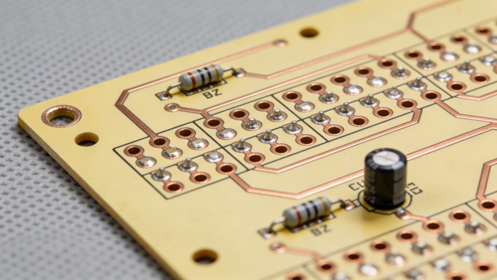
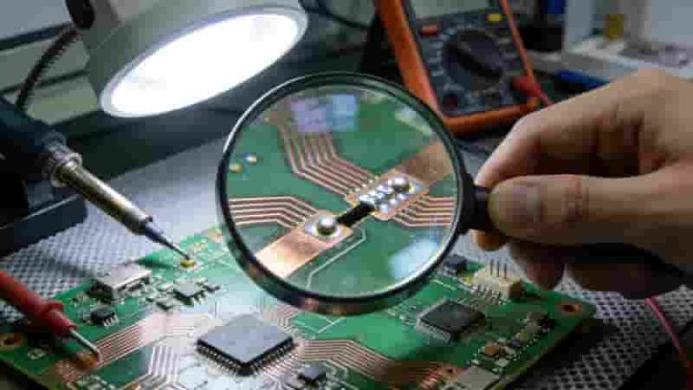
Flying Probe Testing for PCB Bare Board

How Does Flying Probe Testing Work?

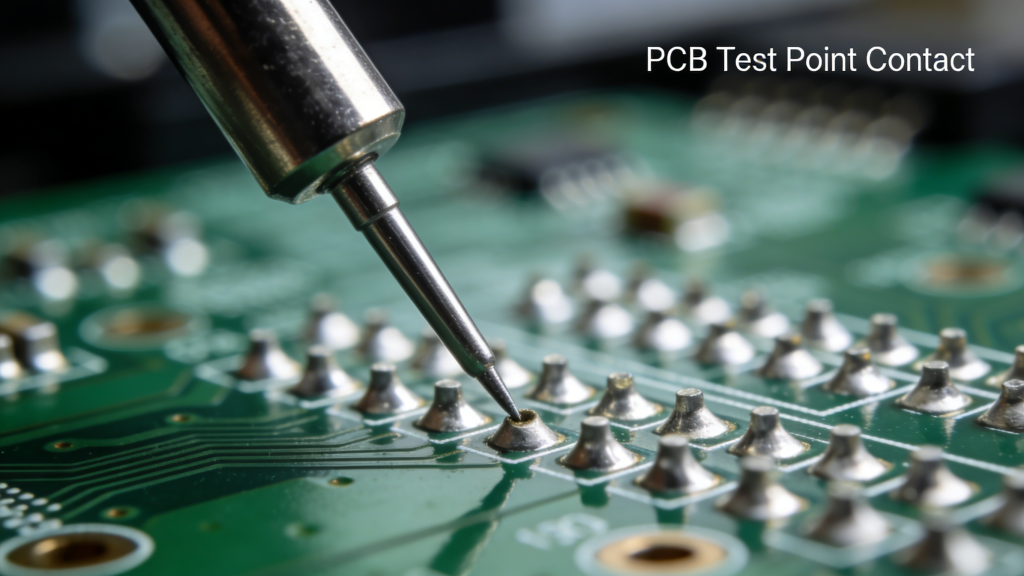
The process begins with importing Gerber, BOM and centroid files to generate a test program. The system then moves precision probes to target pads and test points automatically.

The tester applies low-voltage signals, measures resistance, capacitance and diode voltage, then compares real-time data with standard parameters to judge pass or failure. Defective boards are marked with precise fault locations for repair analysis.
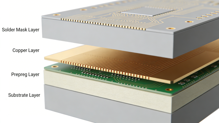
Flying Probe Tester Working Principle

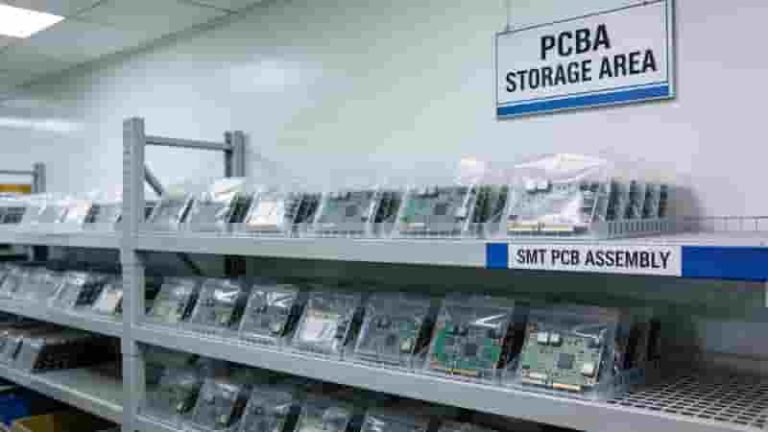
For assembled boards, flying probe testing for PCB also verifies component values, orientation and solder quality, ensuring full functional compliance before mass production.

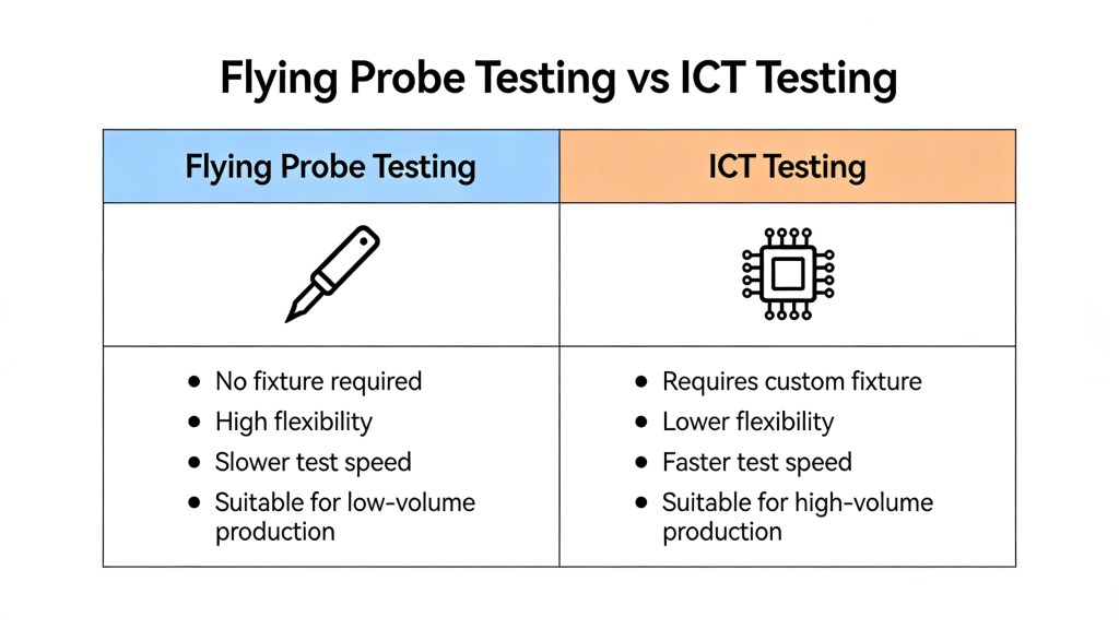
Flying Probe vs ICT Testing

ItemFlying Probe Testing for PCBICT (Bed of Nails)
Fixture RequiredNoYes (High Cost)
Lead TimeFast (Hours/Days)Slow (Weeks)
Best ForPrototypes & Low VolumeHigh Volume Production
Test SpeedMediumVery Fast
Upfront CostLowHigh

Advantages of Flying Probe Testing

  • No expensive fixture, ideal for flying probe testing for PCB prototypes
  • Short setup time, supports rapid engineering iterations
  • High accuracy for opens, shorts and component defects
  • Supports high-density boards (HDI) with small pads
  • Flexible program editing for design changes
  • Compatible with bare boards and assembled PCBA
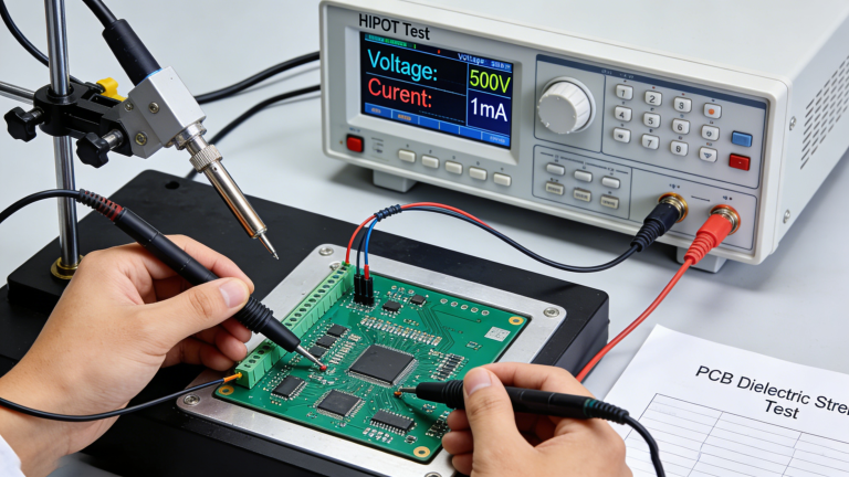
Advantages of Flying Probe Testing for PCB

Limitations

Although flying probe testing for PCB is powerful, it is less efficient for mass production because probes test points sequentially. For high-volume orders, ICT or functional testing is more cost-effective.

It also cannot perform simultaneous multi-point functional testing compared to dedicated fixture-based systems.

Ideal Applications

Flying Probe Testing for PCB is widely used in:

  • PCB prototypes and R&D samples
  • Low-volume & high-mix production
  • High-density interconnect (HDI) boards
  • Pre-mass production verification
  • Reverse engineering and failure analysis
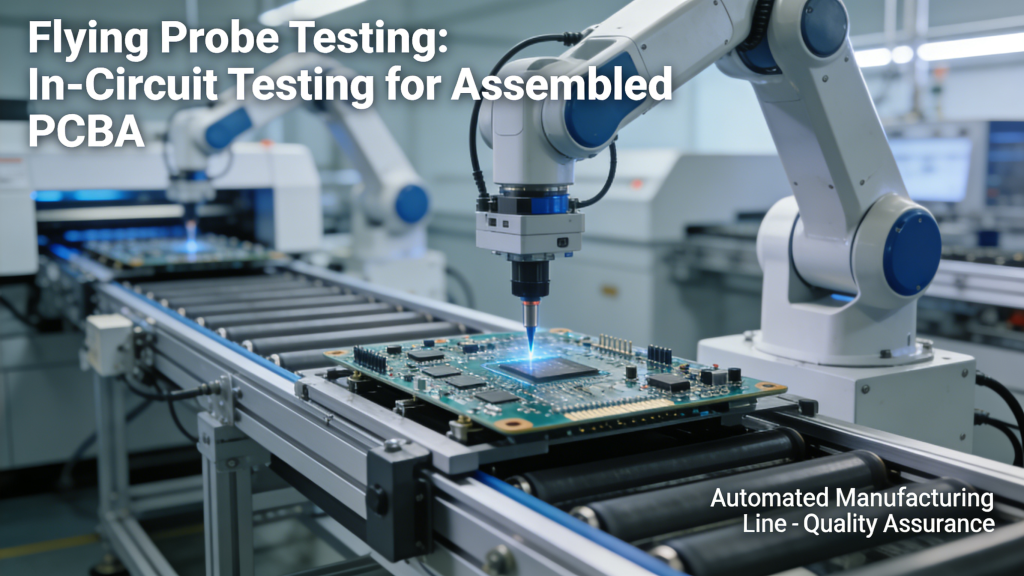
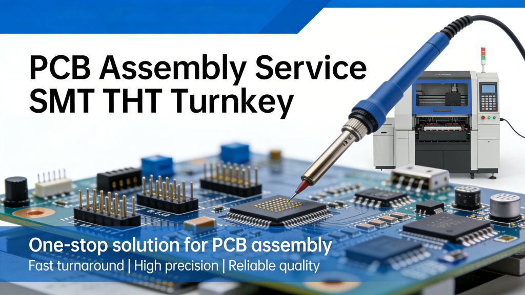
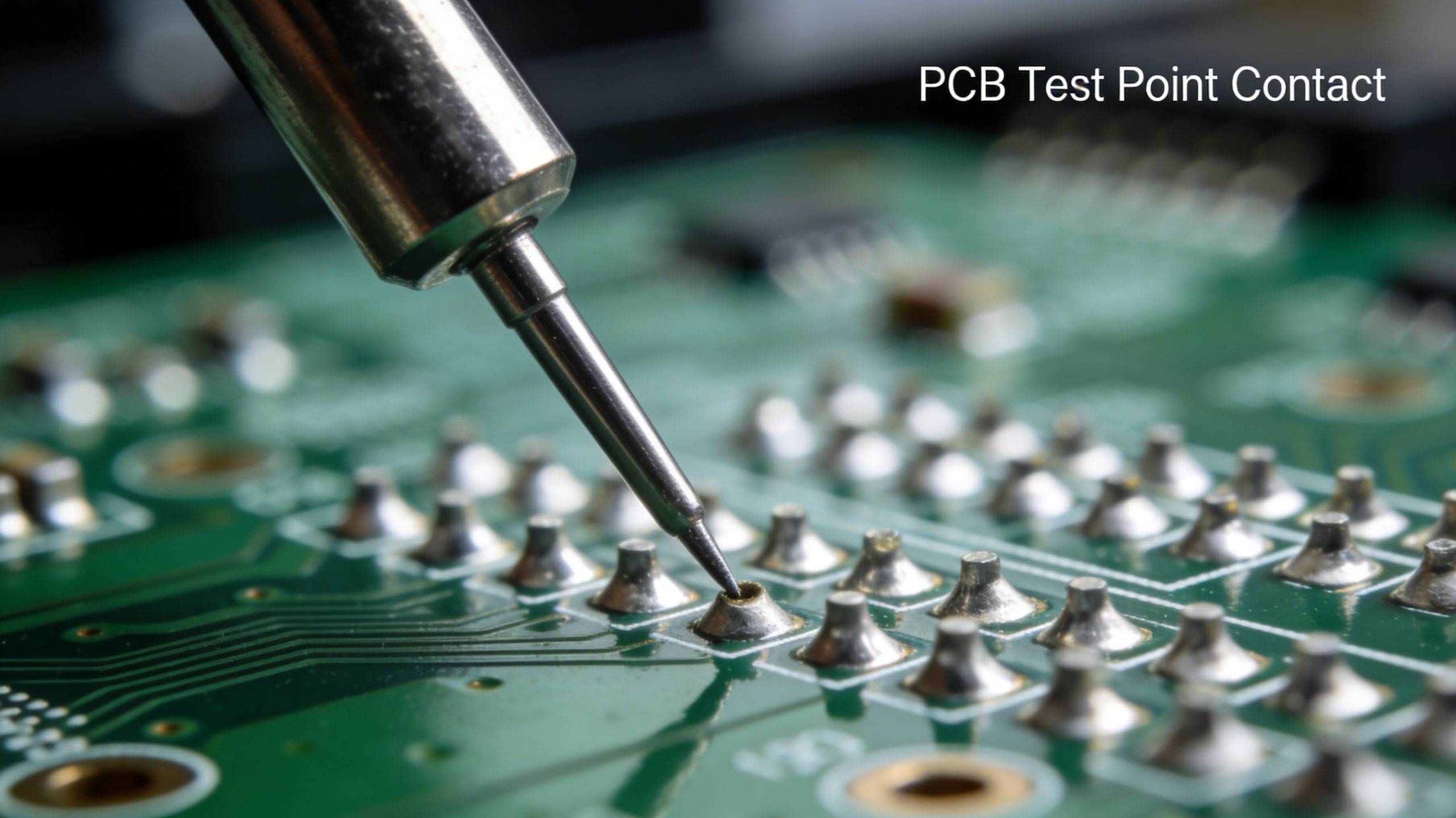
Flying Probe Testing for PCBA Assembly

Conclusion

Flying Probe Testing for PCB remains the most practical and cost-efficient solution for prototype, small-batch and high-mix PCB manufacturing. It eliminates fixture cost, speeds up validation and ensures high reliability without compromising quality.

For projects requiring speed, flexibility and zero fixture investment, flying probe testing is the industry standard choice.

Need Professional Flying Probe Testing for Your PCB?

We provide reliable, fast and cost-effective flying probe testing for PCB and PCBA. Get a free quote and DFM analysis today.

Request a Quote
Flexible PCB fabrication, FPC manufacturing capabilities

PCB Manufacturing Capabilities

Posted on
0 Comments
We continuously upgrade PCB manufacturing processes to maintain our core competitive advantage. Our enhanced capabilities deliver cutting-edge production technologies while reducing total costs for global industrial buyers, engineers, and procurement teams. Full Technical Capabilities of Our PCB Manufacturing & SMT Assembly Services We support full-cycle production for all standard and advanced PCB types, paired with…
China Custom PCB Manufacturer Factory Production Line

China Custom PCB Manufacturer – Full-Service PCB Manufacturing & Assembly

Posted on
0 Comments
As a top China custom PCB manufacturer, we deliver high-precision, cost-effective custom PCB manufacturing for prototypes to mass production. With certified facilities, strict quality control, and global delivery, we support industrial, automotive, medical, and consumer electronics projects worldwide. The Importance of Custom PCB Manufacturing for Electronics Innovation Consumer electronics, industrial equipment, and automotive systems increasingly…
HDI PCB Microvia, Blind & Buried Via Structure

HDI PCB Manufacturing – Microvia, Blind & Buried Via HDI Boards up to 30 Layers

Posted on
0 Comments
HDI PCB manufacturing provides high-density interconnect solutions with microvia, blind via, and buried via structures for compact, high-performance electronics. We deliver reliable HDI boards from prototype to mass production, supporting up to 30 layers for automotive, 5G, medical, and industrial applications. What Is HDI PCB and Why Choose It High-density interconnect (HDI) PCBs offer much…
Plated Through Hole PTH Structure in PCB

What is the Difference Between PTH and Via in PCBs?

Posted on
0 Comments
Understanding the key differences between PTH and via is essential for optimizing PCB design and manufacturing. This article defines PTH and via, compares dimensions, functions, locations and finishing requirements. Typical applications and design considerations are also discussed. Defining PTH and Vias in PCBs PCBs serve as the foundation for almost all modern electronics. They provide…
CNC milling machine

What is a Blank PCB? Buy Bare Circuit Boards | Layer PCB

Posted on
0 Comments
What is a Blank PCB? A Complete Guide to Bare Circuit Boards A blank PCB (also called a bare PCB) is simply the base of an electronic circuit board—it has no electronic parts (like resistors or chips) soldered on it yet. For anyone new to electronics, think of it as a “blank canvas”: you can…
FR-4 PCB 2025 industry standard material for electronics

Why Choose FR-4 as Your PCB Material in 2025? The Definitive Guide

Posted on
0 Comments
In 2025, FR-4 PCB remains the global leading material for rigid printed circuit boards. It delivers the best balance of electrical performance, mechanical strength, thermal stability, flame resistance, cost efficiency, and mass production compatibility. This guide explains why global engineers and buyers choose FR‑4 for industrial, automotive, IoT, 5G, and EV applications. What Is FR‑4…

FAQs About PCB Flying Probe Testing

A: It is a fixtureless electrical test using movable probes to check bare PCBs and PCBAs for opens, shorts, component errors and solder defects.

A: Flying probe needs no fixture, low cost and fast setup for prototypes; ICT requires custom fixtures and works best for high-volume production.

A: It finds open circuits, short circuits, wrong components, reversed polarity, missing parts and bad solder joints.

A: It is ideal for PCB prototypes, low-volume, high-mix orders, HDI boards and pre-production verification.

A: It tests sequentially with medium speed, so it is not efficient enough for large-scale mass production.

A: You need Gerber files, BOM list and centroid files to generate the corresponding test program.

Similar Posts