PCB prototype manufacturing is the critical first step in electronic product development. This professional guide covers full processes, materials, DFM, testing, standards, and selection tips to help you build reliable, production-ready prototypes efficiently.
Introduction to PCB Prototypes
PCB prototype manufacturing validates design functionality, optimizes performance, and reduces risks before mass production. For engineers and procurement teams, high-quality prototypes ensure products meet performance, reliability, and cost targets.
What Is a PCB Prototype?
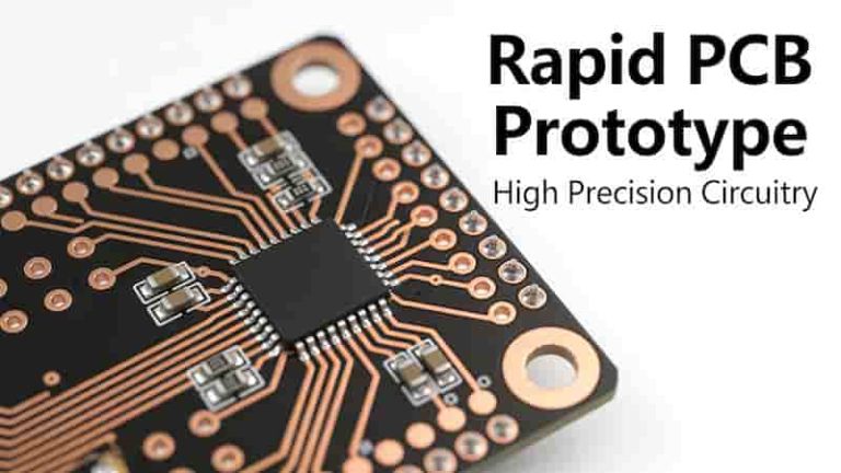
A PCB prototype is a preliminary circuit board used to test design feasibility, electrical performance, and mechanical fit. It helps detect flaws early, cutting development time and lowering overall costs.
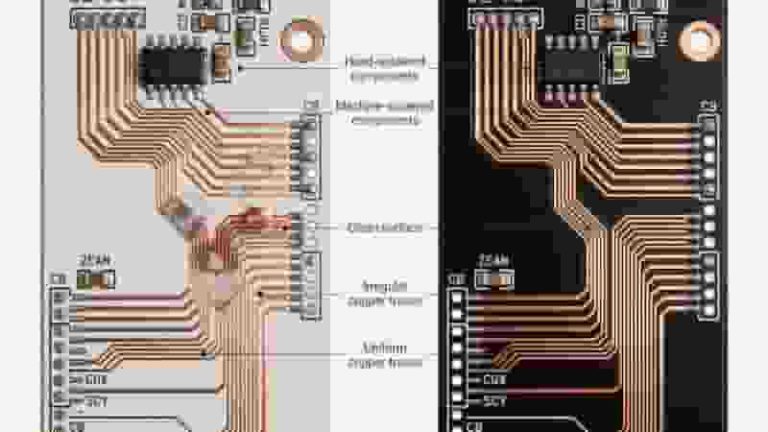
PCBs use etched copper on insulating substrates to connect components. Prototypes replicate final production behavior to validate real‑world performance.
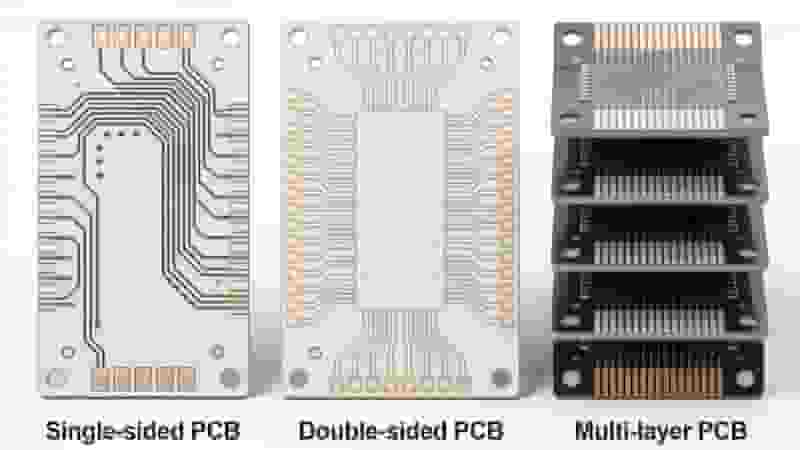
Types of PCB Prototypes
Single‑sided PCB Prototypes – Components and traces on one side; ideal for simple circuits.
Double‑sided PCB Prototypes – Traces on both sides connected by vias; balanced density and cost.
Multi‑layer PCB Prototypes – Stacked inner layers for high‑density electronics; used in industrial and smart devices.
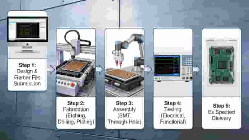
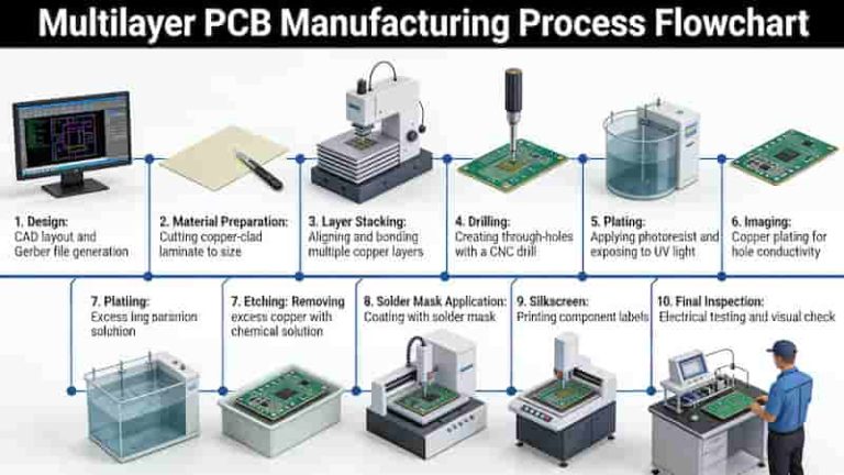
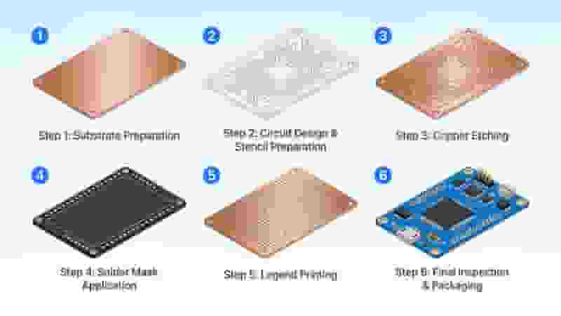
Full PCB Prototype Manufacturing Process
1. Design & File Preparation: CAD layout, Gerber files, DFM check.
2. Printing & Photomask: Transfer design to the substrate.
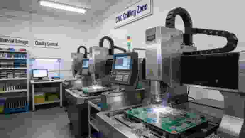
3. Drilling: Precision holes for vias and components.
4. Plating: Copper deposition for conductive paths.
5. Etching: Remove excess copper to form circuits.
6. Solder Mask & Silkscreen: Protection and labeling.
7. Surface Finish: HASL, ENIG, OSP, etc.
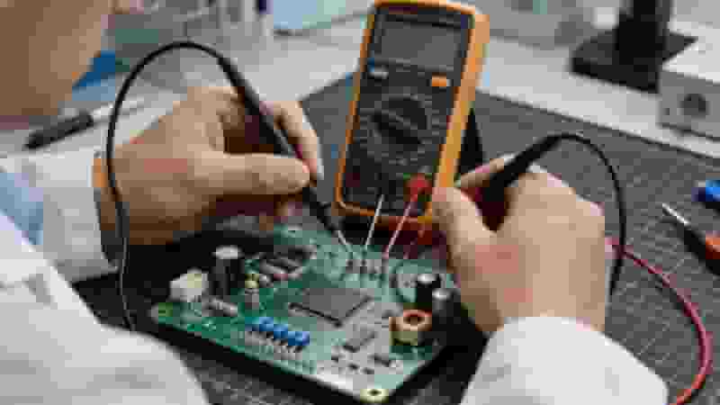
8. Electrical Testing & Assembly: Functional verification.
Materials & Specifications
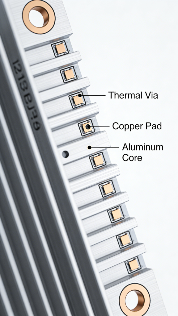
Common substrates: FR‑4, High‑Tg FR‑4, Aluminum, Rogers, Flexible PI.
Copper thickness: 1/3oz to 2oz.
Trace width / spacing: Down to 3mil / 3mil for high‑density designs.
DFM Guidelines for PCB Prototypes
Optimize tolerances for PCB prototype manufacturing stability.
Standardize via size and annular rings.
Avoid overly complex structures that raise cost and lead time.
Testing & Quality Control
AOI – Automated Optical Inspection
Electrical continuity & isolation test
Impedance test (for high‑frequency boards)
Thermal & reliability validation
How to Choose a PCB Prototype Manufacturer
• Technical capability for PCB prototype manufacturing
• Quality system & certification
• Quick turnaround (24hr–5days)
• Competitive pricing
• Responsive engineering support
Our PCB Prototype Manufacturing Services
We provide full‑service PCB prototype manufacturing for global industrial buyers and engineers.
Supported types: Single‑sided, double‑sided, multilayer up to 20 layers
Surface finishes: HASL, ENIG, OSP, Immersion Silver, Gold Finger
Solder mask colors: Green, black, red, white, blue, yellow
Turnaround: Quick‑turn options as fast as 24 hours
Assembly: SMT & through‑hole prototype assembly available
Summary
PCB prototype manufacturing is foundational to successful electronic development. Working with an experienced partner ensures reliable, on‑time, cost‑effective prototypes that accelerate your product launch.
Get Your PCB Prototype Quote Today
Send us your Gerber files and requirements for a free, fast quotation on PCB prototype manufacturing. We support quick‑turn, high‑quality, and fully customized solutions for global buyers.
Inquire Now | Custom PCB Prototype
Aluminum PCB Manufacturing Process: Step-by-Step Guide
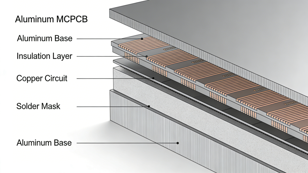
Metal Core PCB (MCPCB) Manufacturing Service in China
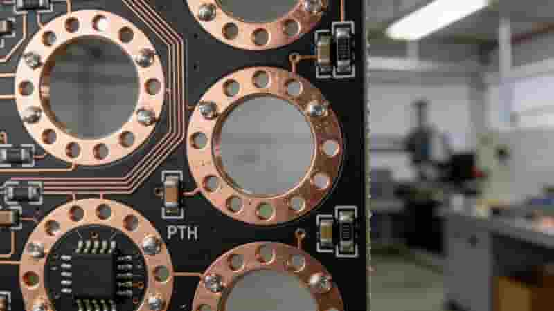
Understanding Plated Through Holes (PTH) for Printed Circuit Boards
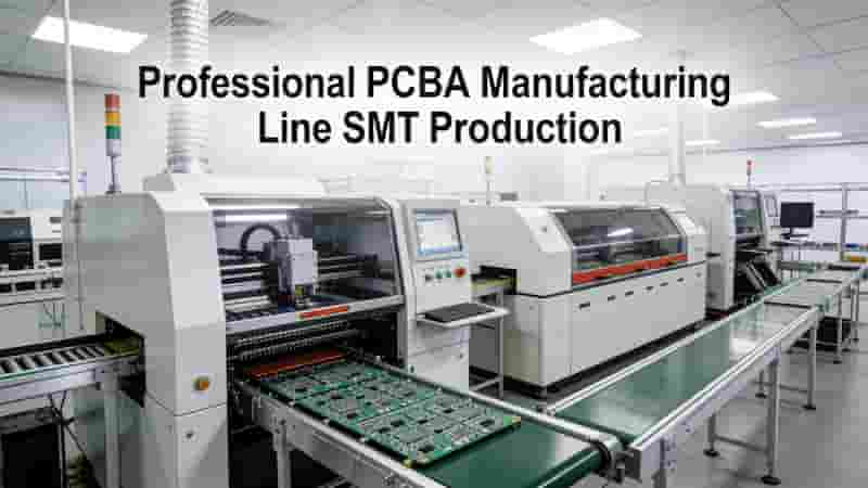
Printed Circuit Board Assembly Services | Full Turnkey PCBA Solutions
Professional LED PCB Manufacturing & Assembly Services