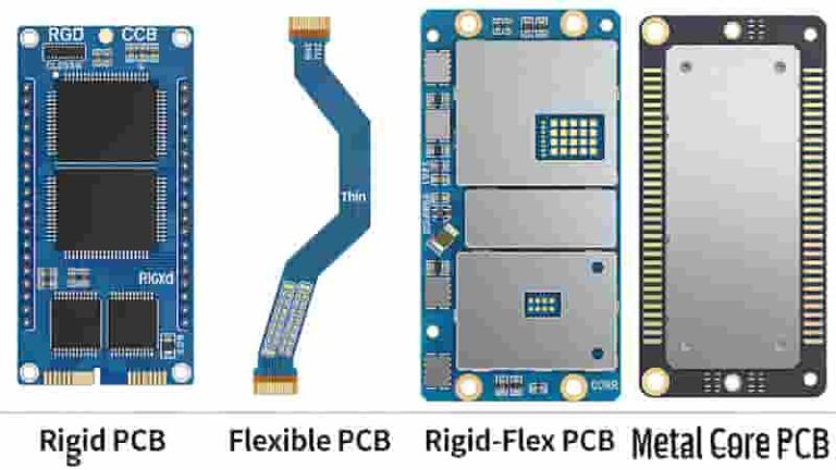
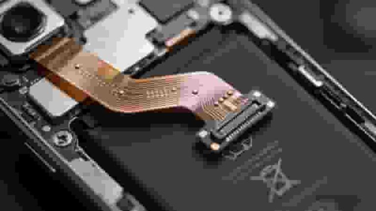
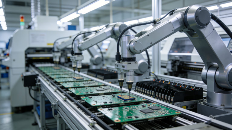
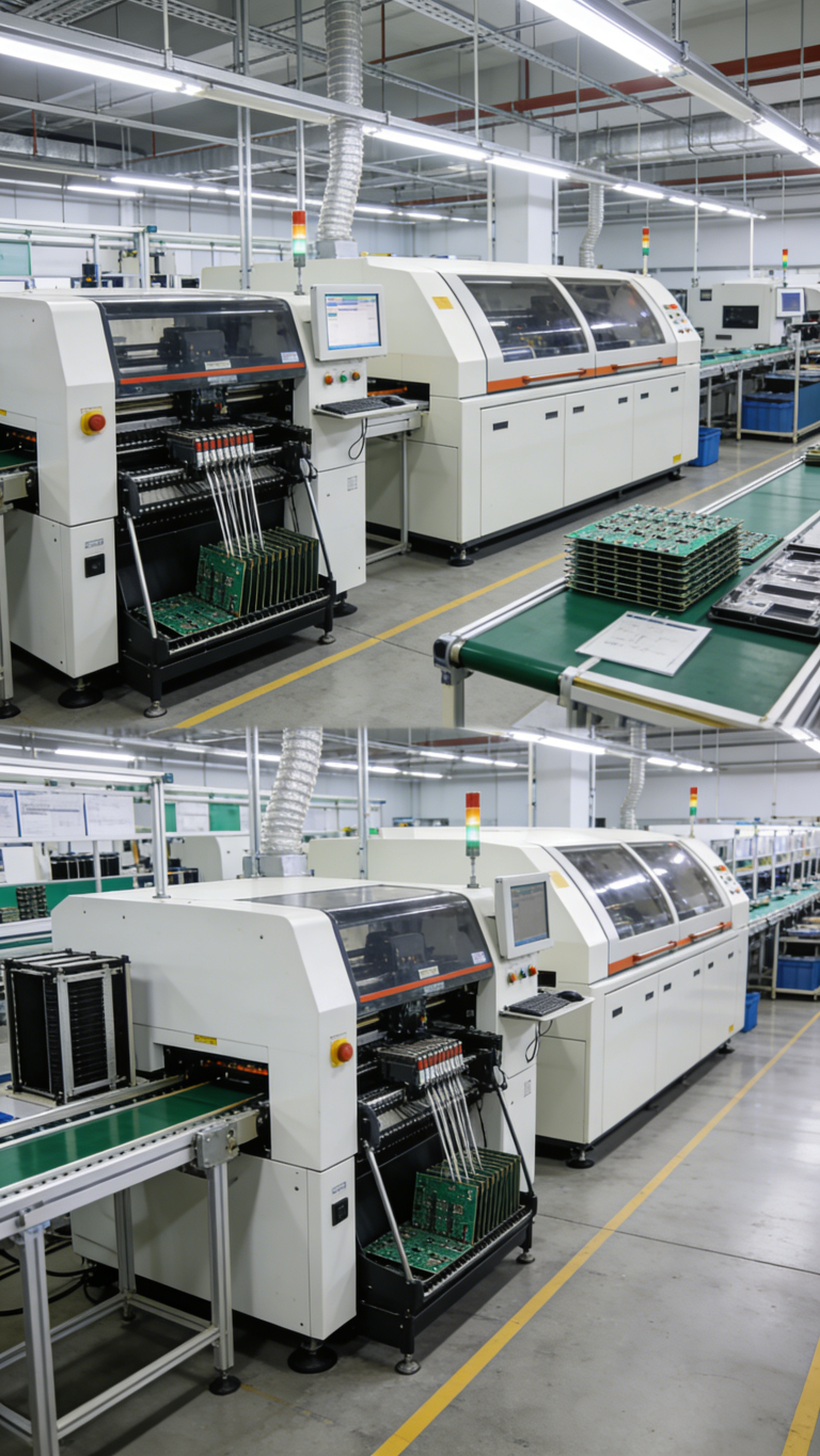
We provide custom single-layer, double-sided, and multilayer flexible PCB solutions for prototyping and mass production. As a professionalflex PCB manufacturer, we deliver fast turnaround, stable quality, and full engineering support for global industrial buyers, engineers, and procurement teams.
Flexible PCB Manufacturing Capabilities
We specialize in full‑service flex PCB fabrication from simple prototypes to complex high‑volume production. Our capabilities cover single‑layer, double‑sided, multilayer flexible PCB and rigid‑flex PCB designs with strict quality standards.
| Item | Specification |
|---|---|
| Layers | 1–12 layers for flex & rigid‑flex PCB |
| Base Material | Polyimide (PI), PET, LCP, high‑performance flex laminates |
| Board Thickness | 0.05 mm – 0.4 mm |
| Min Hole Size | 0.1 mm (laser drilling supported) |
| Surface Finish | ENIG, OSP, Immersion Tin, Hard Gold, Gold Finger |
| Prototype Lead Time | 24–48 hours quick‑turn available |
| Certifications | ISO 9001, IATF 16949, UL, IPC‑A‑600 |
Types of Flexible PCBs We Provide
We design and manufacture a full range of flexible PCB types to match your prototype and production requirements.
Single Layer Flexible PCB
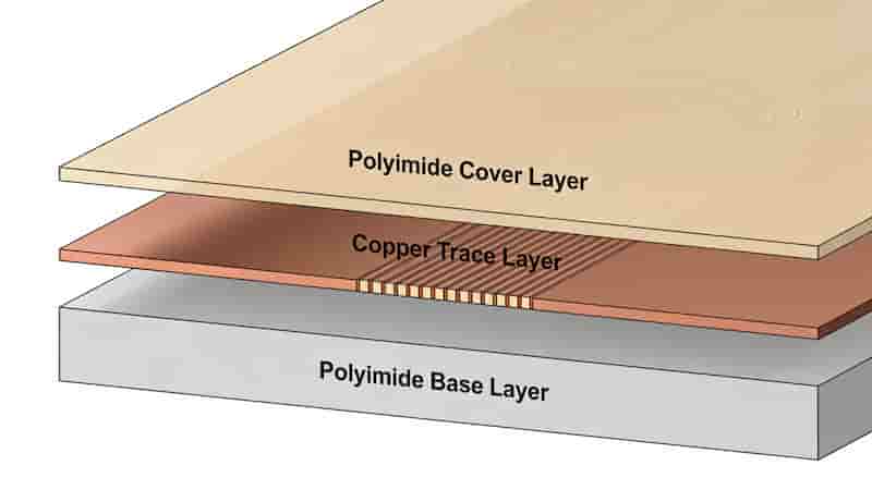
Single‑layer flex PCB uses one copper layer on polyimide base. Ideal for simple interconnections, LED strips, and cost‑effective devices with basic routing needs.
Double Sided Flex PCB
Double‑sided flexible PCB features copper on both sides with plated through holes. It supports higher component density and more complex circuit layouts.
Multilayer Flex PCB
Multilayer flex PCB stacks three or more conductive layers with insulating films. Suitable for high‑density, impedance‑controlled, and dynamic bending applications.
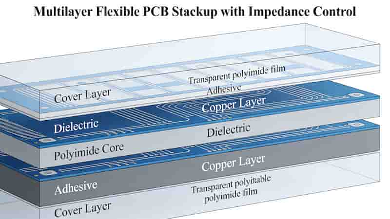
Rigid‑Flex PCB
Rigid‑flex PCB combines rigid FR4 sections and flexible layers into one integrated unit. It reduces connectors, improves reliability, and fits space‑constrained mission‑critical products.
Flexible PCB Industry Applications
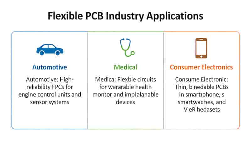
Our flex PCB fabrication serves global industries that require thin, lightweight, and reliable interconnect solutions.
Consumer Electronics: Smartphones, tablets, cameras, wearables, and home devices with limited space.
Medical & Wearable Devices: Body‑friendly sensors, portable monitors, and implantable support equipment.
Automotive & Industrial Electronics: Control modules, instrument clusters, and devices used in high‑vibration environments.
Telecom & Data Communication: High‑speed signal modules, antennas, and networking equipment.
Why Choose Us as Your Flex PCB Manufacturer
We are a trusted flexible PCB manufacturer focused on quality, speed, and customer success for global export markets.
Quick‑Turn Prototypes: 24/48H fast lead time for flex PCB samples to speed up your design validation.
Stable Quality System: Full in‑process inspection and reliability testing ensure consistent performance.
Professional Engineering Support: DFM review, stack‑up design, and material selection to optimize your design.
Cost‑Effective Production: Scalable capacity and efficient supply chain for competitive pricing.
Flex PCB Manufacturing Process & Quality Control
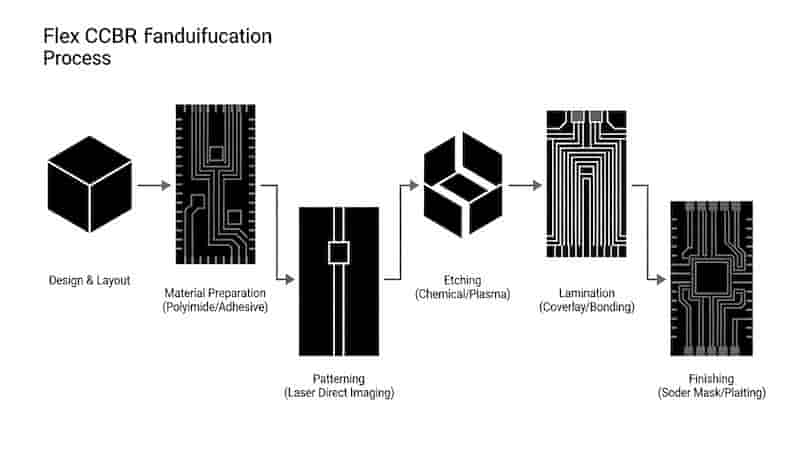
Our standardized flex PCB fabrication process ensures high yield and reliable quality for every order.
1. Material Preparation: Incoming inspection for flex laminates, coverlay, and copper materials.
2. Drilling & Plating: Precision drilling and copper plating for stable interlayer connections.
3. Imaging & Etching: High‑precision circuit transfer and controlled etching.
4. Coverlay & Surface Finish: Protective lamination and surface treatment for solderability.
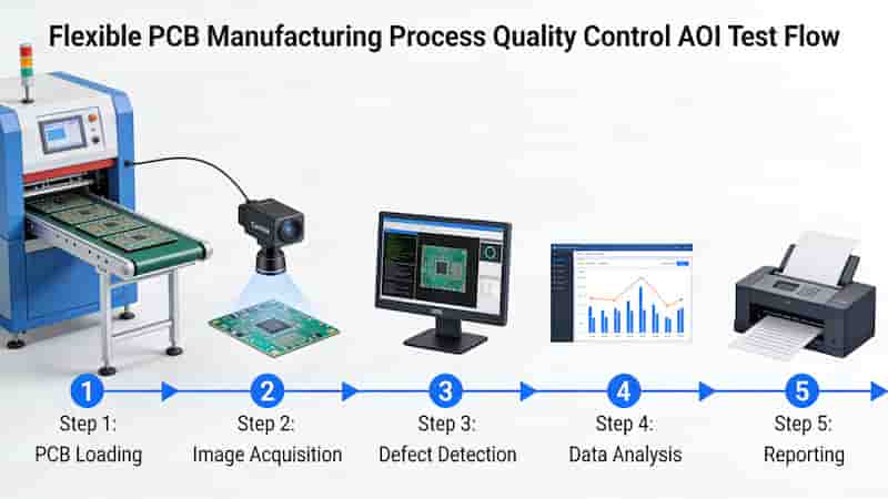
5. Final Testing: AOI, electrical test, and reliability verification before shipment.
Summary
As a professional flexible PCB manufacturer, we deliver reliable flex PCB fabrication for single‑layer, double‑sided, multilayer, and rigid‑flex designs. With fast turnaround, strict quality control, and full engineering support, we help global customers build high‑performance flexible circuits for prototyping and mass production.
Request a Custom Flex PCB Quote
Get a fast, accurate quote for your flexible PCB project. Send your Gerber files, layer count, quantity, material, and surface finish requirements, and we will respond quickly with pricing and lead time.
Get Your Flex PCB Quote Today
Upload Gerber Files • Send Specifications • 24H Quick Response • Global Delivery
PCB Materials Classification & Substrate Selection Guide
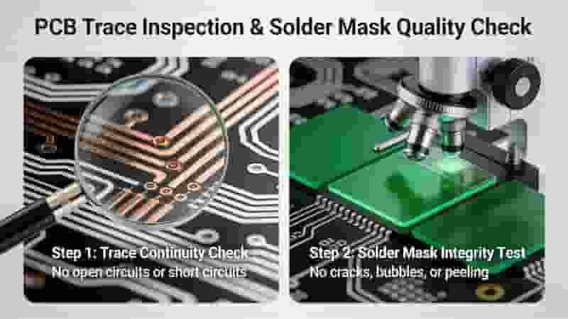
How to Judge PCB Quality: 7 Expert Tips for Reliable Boards
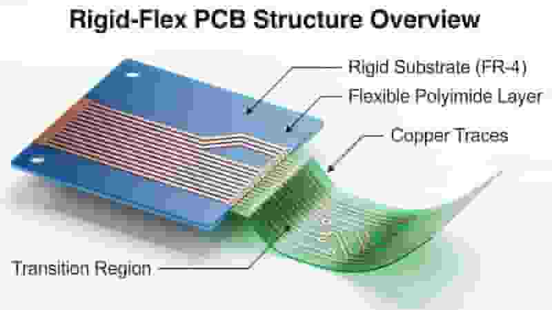
Ultimate Guide to Rigid-Flex PCB Manufacturing: Process, Materials & Quality
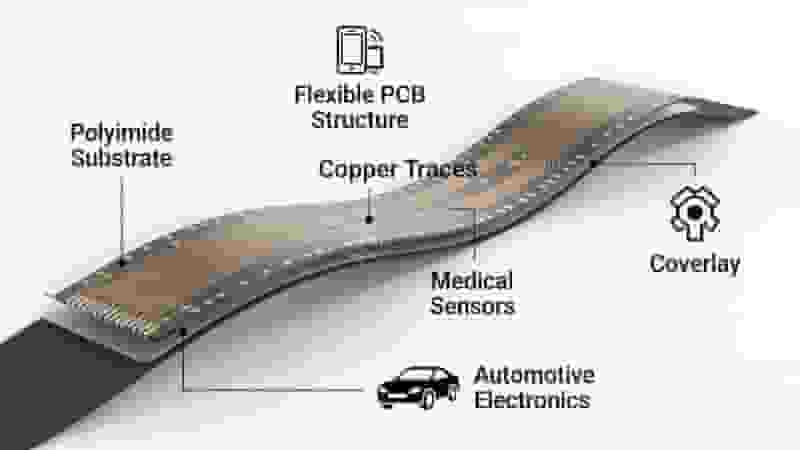
Flexible PCB Manufacturing Process Steps: Complete Technical Guide
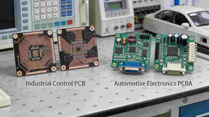
What Is the Difference Between PCB and PCBA? A Complete Guide for Industrial Buyers