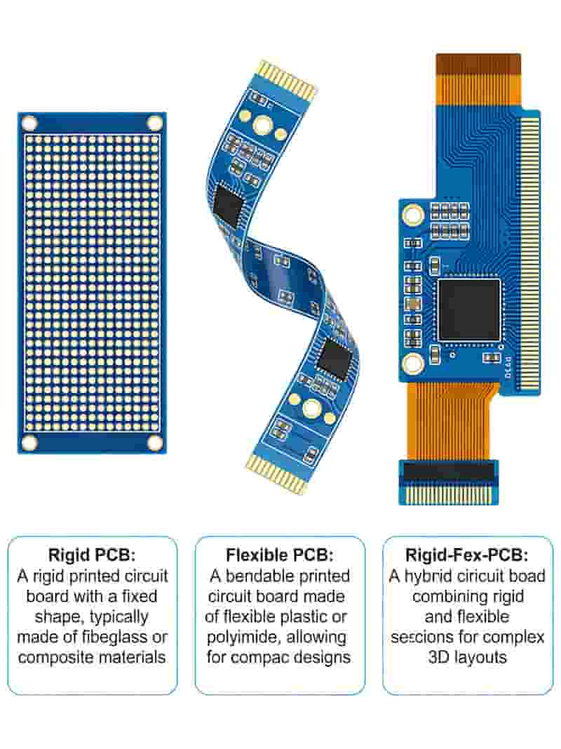
|

PCB Manufacturing Capabilities

Flexible PCB fabrication, FPC manufacturing capabilities

We continuously upgrade PCB manufacturing processes to maintain our core competitive advantage. Our enhanced capabilities deliver cutting-edge production technologies while reducing total costs for global industrial buyers, engineers, and procurement teams.

Full Technical Capabilities of Our PCB Manufacturing & SMT Assembly Services

We support full-cycle production for all standard and advanced PCB types, paired with reliable SMT assembly for prototype through mass-production orders.

Rigid Printed Circuit Boards

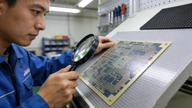
Rigid PCB Manufacturing Capabilities

  • Layers: 1-30
  • MOQ: 1 pc
  • Materials: FR4, Aluminum, etc.
  • Laminate: Shengyi, Isola, etc.
  • Thickness: 0.1-8.0 mm
  • Max Size: 533.4 × 762 mm
  • Lead Time: 24 Hours – 9WD
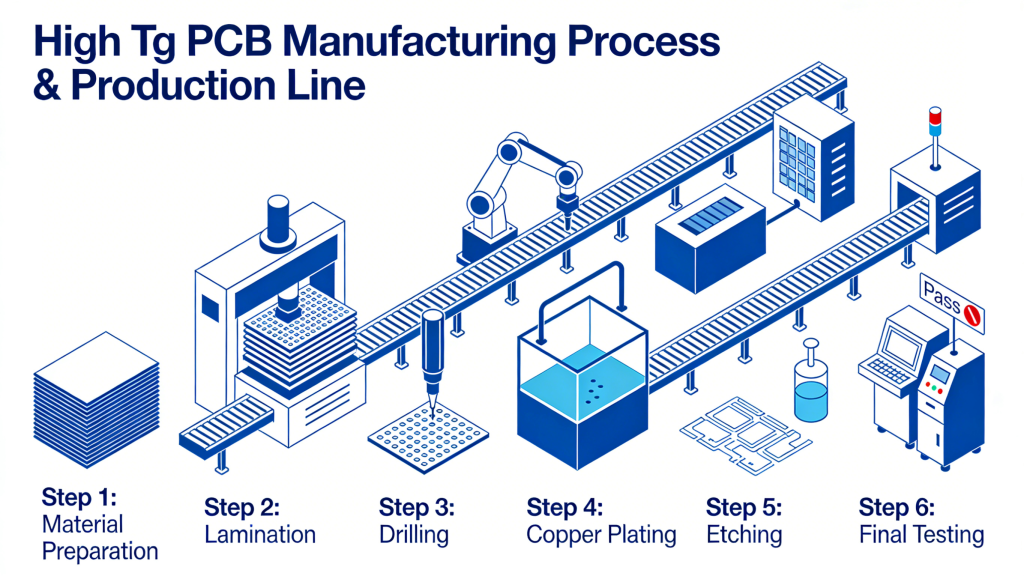
  • Types: LED PCB, HDI PCB, Flexible PCB, Rigid-flex PCB, High Tg PCB, etc.
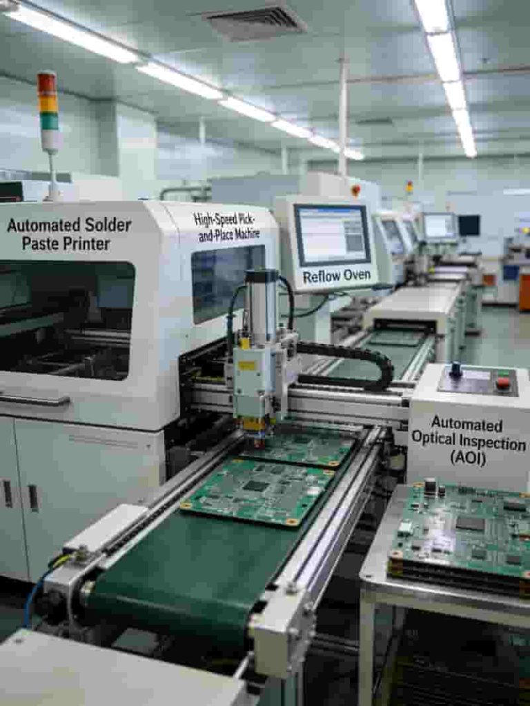
Rigid PCB manufacturing capabilities, multilayer PCB production

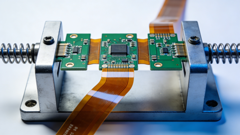
Flexible Printed Circuit Boards

Flexible PCB Fabrication Capabilities

  • Layers: 1-10
  • MOQ: 1 pc
  • Laminate: Dupont PI, Shengyi PI
  • Minimum Hole Size: 0.1 mm
  • Thickness: 0.05 mm ±0.02 mm
  • Max Size: 480 × 4000 mm
  • Panelization Size: 250 × 510 mm
  • Lead Time: 24 Hours – 9WD
  • Solder Mask Color: Green, White, Blue, Black, Red, Yellow, etc.
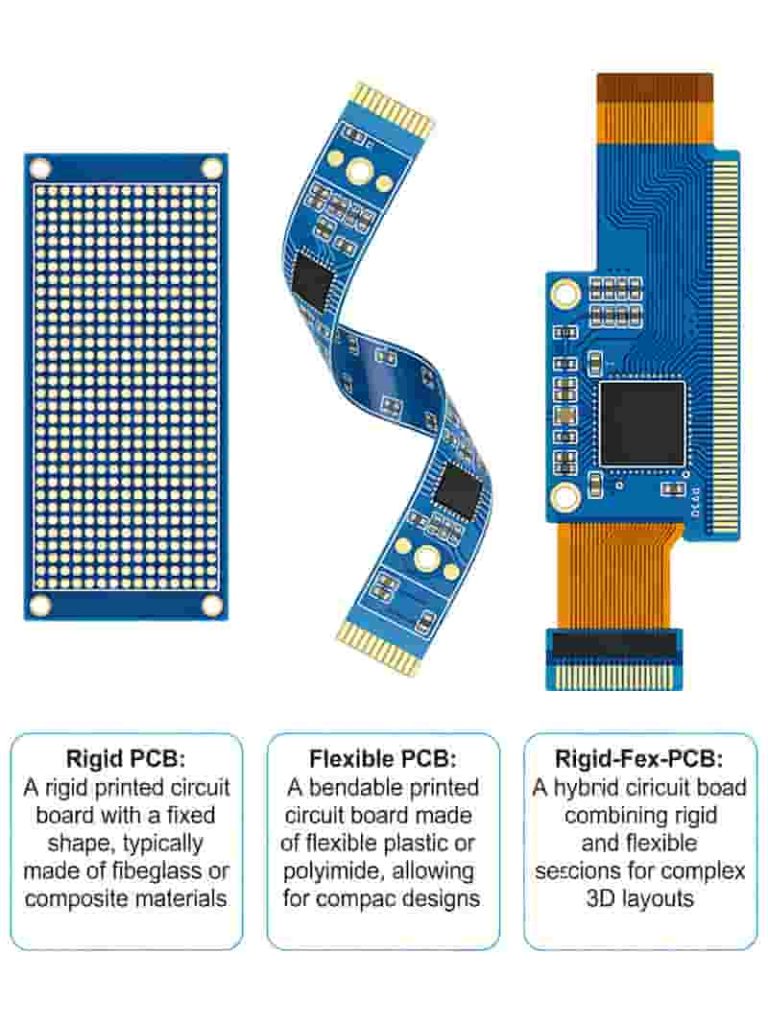
Flexible PCB fabrication, FPC manufacturing capabilities

Rigid-Flex Printed Circuit Boards

Rigid-Flex PCB Fabrication Capabilities

  • Layers: 1-12
  • Laminate: Dupont PI, Halogen Free
  • Thickness: 0.20 – 5.50 mm
  • Max Size: 610 × 640 mm
  • Impedance Control: ±10%
  • Surface Finish: HASL (LF), ENIG, Immersion Tin/Silver
  • Solder Mask Color: Green, White, Blue, Black, Red, Yellow, etc.
Rigid-flex PCB manufacturing, high reliability rigid flex boards

High Density Interconnector (HDI) PCBs

HDI PCB Manufacturing Capabilities

  • Layers: 4-24
  • MOQ: 1 pc
  • HDI Structures: 1+N+1, 2+N+2, 3+N+3
  • Quality Grade: Standard IPC 2
  • Build Time: 2 days – 5 weeks
  • Material: FR4 standard Tg 140°C | FR4 High Tg 170°C, etc.
  • Board Size: Min 6×6 mm | Max 457×610 mm
  • Board Thickness: 0.4 mm – 3.0 mm
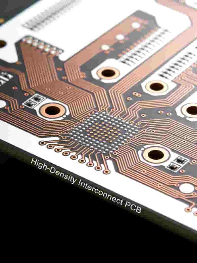
HDI PCB manufacturing capabilities, high density interconnect PCB

PCB SMT Stencil Manufacturing

PCB Stencil Fabrication Capabilities

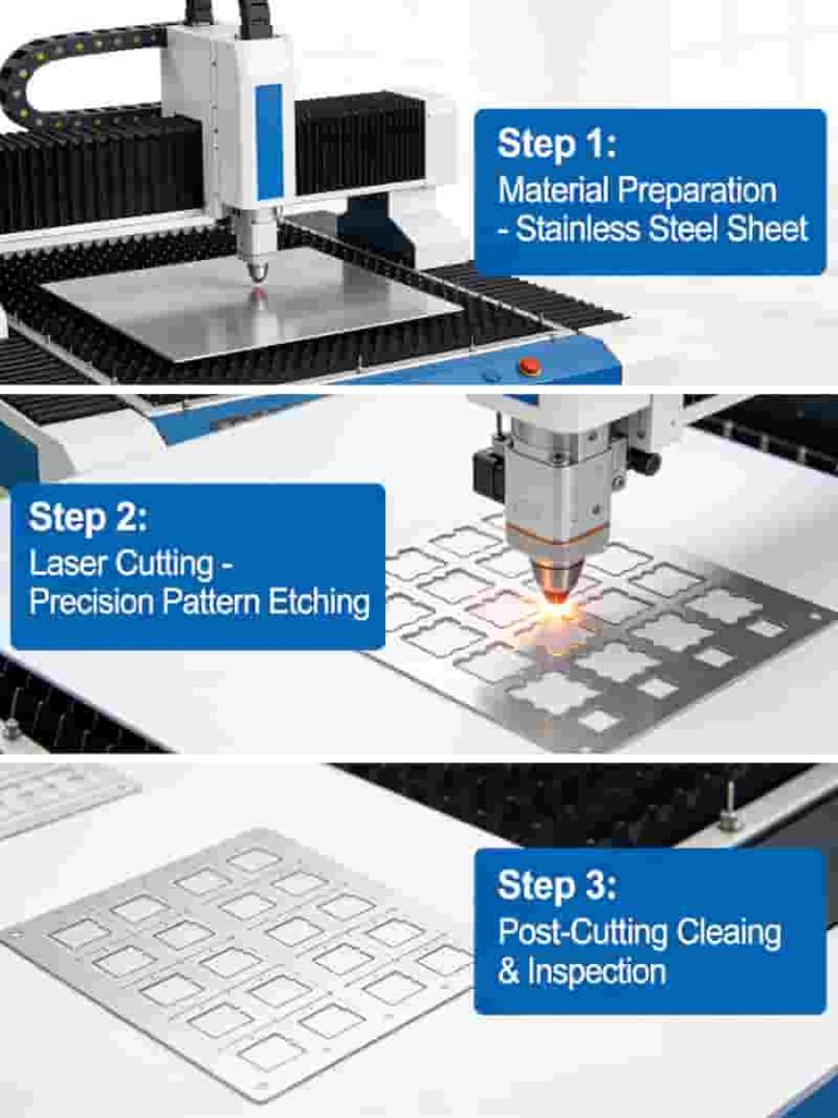
  • Technology: 100% laser cut
  • Types: Framed, Frameless, Electroformed, Nano Coating
  • Material: Stainless Steel
  • Stencil Thickness: 0.06 ~ 0.3 mm
  • Minimum Cut Width: 0.05 mm
  • Maximum Size: 736 × 736 mm
  • Aperture Tolerance: within 0.007 mm
  • Fiducial Data Support: Yes
  • Panelized Data Support: Yes
  • Delivery: 1-2 days
SMT stencil manufacturing, laser cut PCB stencils

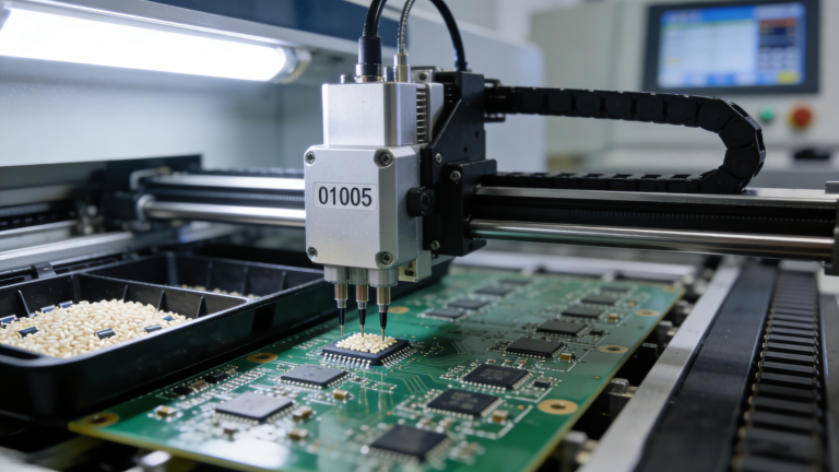
PCB Assembly (PCBA) Services

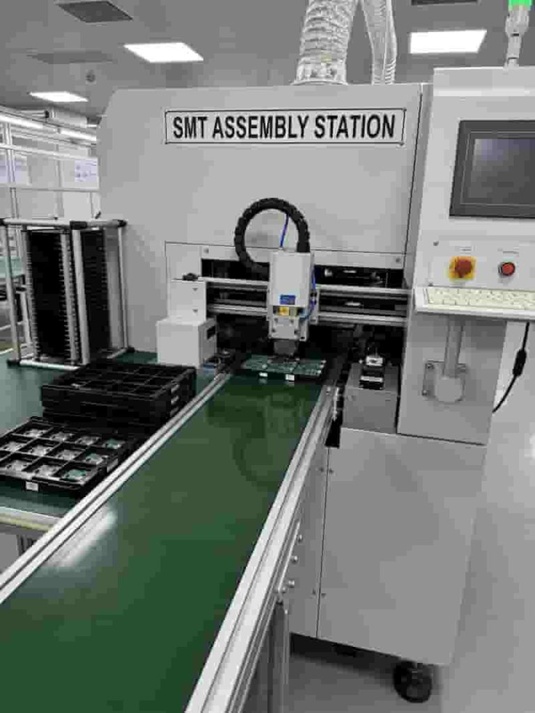
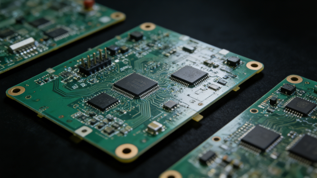
PCB Assembly PCBA Capabilities

  • PCB Types: Rigid, Flexible, Rigid-flex, Multilayer, etc.
  • PCB Size: 50×50 mm – 774×710 mm
  • Material: Rigid | Metal Core | FPC
  • Shape: Any custom shape
  • Quantity: Prototype to high volume, no MOQ
  • Services: Quick-turn prototype assembly, full turnkey solutions

PCB Type Comparison

PCB TypeLayersLead TimeBest For
Rigid PCB1-3024h-9WDGeneral electronics, industrial controls
Flex PCB1-1024h-9WDWearables, compact devices
HDI PCB4-242d-5wHigh-tech, miniaturized products

Conclusion

Our full-spectrum PCB manufacturing capabilities enable us to support projects from early prototype to large-scale global export. We combine advanced processes, strict quality control, and fast lead times to help you reduce costs and speed up time to market.

Ready to Start Your PCB Projects?

Get DFM-optimized boards in as fast as 24 hours. 100% quality guaranteed for global export.

Get a Free Quote
Email Us
SMT PCB Assembly Defects Overview - Common Soldering and Placement Issues

30 Common SMT PCB Assembly Defects: Causes, Impacts & IPC-Compliant Prevention

Posted on
0 Comments
This professional guide covers the top 30 SMT PCB assembly defects, their root causes, quality risks, and proven fixes to boost yield and reliability for industrial buyers and engineers. 1. Soldering & Solder Joint Defects Solder joints are the foundation of reliable SMT PCB assembly. Even minor flaws cause intermittent failures or early breakdowns. 1….
Step-by-step PCB via manufacturing: drilling, plating, filling and capping

PCB Vias: Complete Guide to Types, Design, Reliability and Performance

Posted on
0 Comments
A full professional overview of PCB vias including definitions, functions, types, manufacturing, reliability factors and advanced technologies for high‑performance multilayer printed circuit boards. Introduction: Definition, Role, and Types of Vias in PCBs A via is a vertical electrical connection between layers in a printed circuit board. Vias enable traces to transition between layers to facilitate…
Affordable PCB Prototyping Benefits for Engineers and Startups

Why Choose Affordable PCB Prototyping?

Posted on
0 Comments
Affordable PCB prototyping helps engineers, startups and manufacturers validate designs quickly, cut development costs, avoid mass-production risks and speed up time-to-market without sacrificing quality or reliability. Key Benefits of Affordable PCB Prototyping Choosing affordable PCB prototyping brings measurable business and engineering advantages for every electronics project. Reduce Total Development CostEarly validation with low-cost PCB prototype…
Semi-Flex PCB Bending Principle Depth Milling

Semi-Flex PCBs: The Ultimate Bridge Between Rigid and Flex PCBs

Posted on
0 Comments
Semi-Flex PCBs deliver the ideal balance of rigidity and flexibility for modern electronics. Built on standard FR-4 with precision thinned bending zones, they offer cost efficiency, reliable performance, and easy assembly, filling the critical gap between traditional rigid PCBs and high-cost flex circuits. Ideal for static bend installations, Semi-Flex PCBs reduce assembly complexity while enhancing…
Double-Sided Flex PCB Structure Diagram | Flexible Circuit Layer Structure

Double-Sided Flex PCB Manufacturing Services | 2-Layer Flexible PCB Solutions

Posted on
0 Comments
Double-sided flex PCB (also known as 2-layer flexible PCB) is a flexible circuit with two copper conductive layers on polyimide film, connected by plated through holes. We provide full-process manufacturing, customized stackup, strict quality control and fast delivery for global industrial, medical, automotive and high-tech electronics applications from prototype to mass production. What Is a…
Flexible PCB materials polyimide PET RA copper ED copper

Flexible PCB: Full Guide to Materials, Design & Applications

Posted on
0 Comments
Flexible PCB (FPC/flex circuit) is a thin, bendable printed circuit that fits 3D spaces. This engineering guide covers materials, design rules, manufacturing, types, reliability & industrial uses for global buyers. Modern electronics demand thinner, lighter, higher-density interconnects. Flexible PCB (also called FPC or flex circuit) has become a core technology enabling miniaturization and 3D packaging….

FAQs About Our PCB & PCBA Full Capabilities

A: Rigid PCB: 1–30 layers; Flexible PCB: 1–10 layers; Rigid-flex PCB: 1–12 layers.

A: MOQ is 1 piece, supporting prototype, small batch and mass production orders.

A: We adopt Dupont PI and Shengyi PI as main substrates, with minimum hole size down to 0.1 mm.

A: HDI supports 1+N+1, 2+N+2, 3+N+3 structures, using standard Tg and High Tg FR4 materials.

A: Thickness 0.06~0.3 mm, minimum cut width 0.05 mm, aperture tolerance within 0.007 mm, delivery in 1–2 days.

A: Green, white, blue, black, red, yellow and other custom colors are optional.

A: Rigid and flex PCB: 24 hours to 9 working days; HDI PCB: 2 days to 5 weeks.

A: We assemble rigid, flex, rigid-flex, multilayer and metal core PCBs with no MOQ limit.

Similar Posts