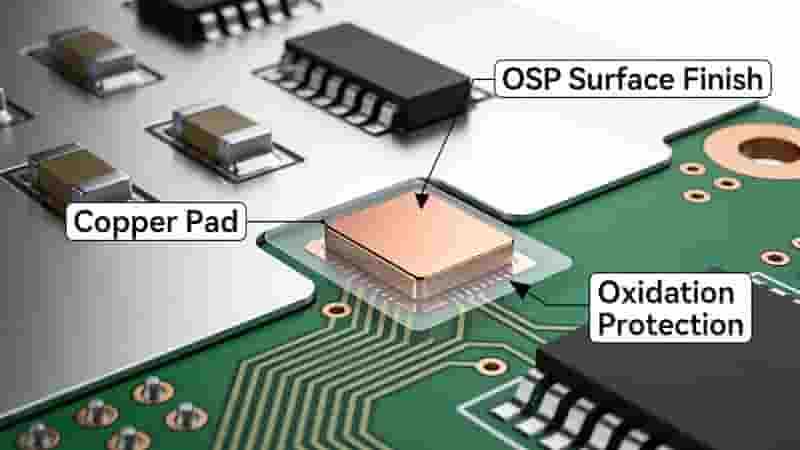
OSP (Organic Solderability Preservative) is a lead‑free, RoHS‑compliant organic coating applied to exposed copper pads on printed circuit boards to prevent oxidation and preserve solderability before SMT assembly. This guide explains PCB OSP surface finish in full: process, pros, cons, storage, assembly, comparisons, and best practices for industrial electronics manufacturing.
What Is PCB Surface Finish?
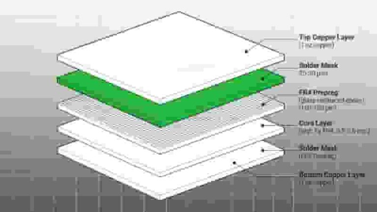
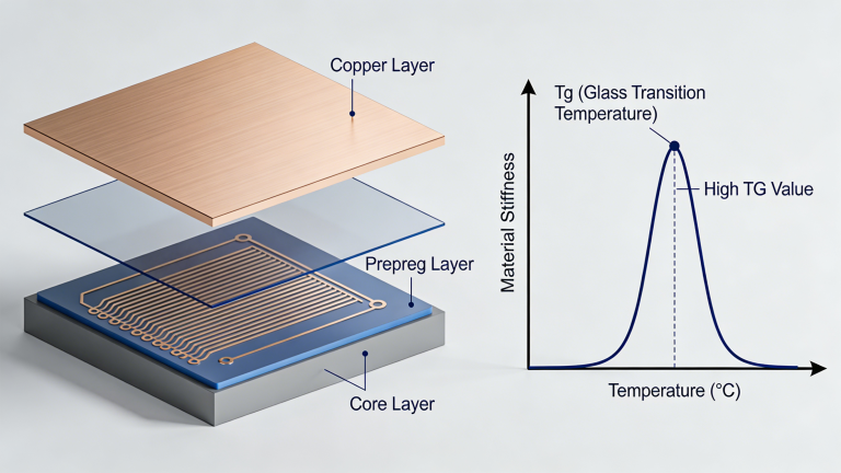
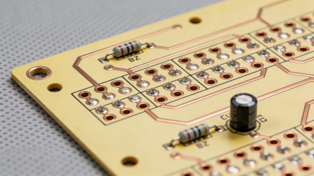
A PCB surface finish is a protective layer applied after solder mask development. It shields exposed copper from oxidation, corrosion, and contamination while providing a stable, solderable surface for component mounting. Surface finishes are divided into metallic types (ENIG, Immersion Silver, HASL) and organic types, with OSP surface finish being the most widely used organic solution.
Key functions include ensuring reliable soldering, extending board life, supporting fine‑pitch SMT assembly, and complying with global environmental regulations such as RoHS and WEEE.
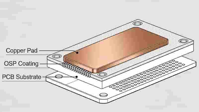
What Is OSP Surface Finish?
OSP (Organic Solderability Preservative) is a water‑based, transparent organic compound that bonds chemically to copper surfaces. It forms a thin protective film that blocks oxidation and preserves solderability without adding metallic layers. This makes PCB OSP finish ideal for lead‑free assembly, high‑yield production, and cost‑sensitive industrial projects.
Unlike ENIG or Immersion Silver, OSP leaves a perfectly flat surface, which is critical for BGAs, QFNs, and other fine‑pitch components used in consumer electronics, automotive, and industrial control systems.
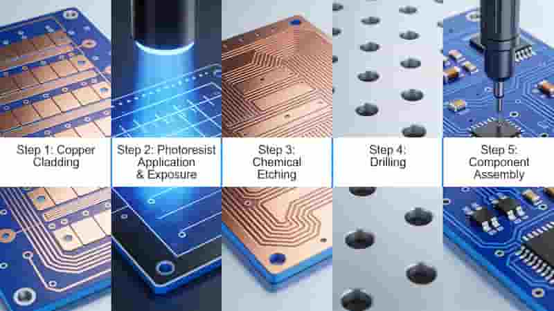
OSP Surface Finish Manufacturing Process
The OSP coating process is clean, efficient, and compatible with high‑volume PCB lines:
- Cleaning: Removes oils, residues, and oxides from copper pads.
- Micro‑Etching: Improves adhesion for the OSP layer.
- DI Rinsing: Eliminates ionic contamination.
- OSP Coating: Uniform organic film deposition at pH 4.0–7.0.
- Drying: Stabilizes the coating for safe handling and storage.
Advantages of OSP Surface Finish
PCB OSP finish offers industry‑leading benefits for mass production:
- Excellent flatness for fine‑pitch and BGA components
- Lowest cost among mainstream surface finishes
- 100% RoHS‑compliant and eco‑friendly
- Simple rework and repair capability
- Compatible with lead‑free reflow and wave soldering
- No heavy metals or hazardous waste
Limitations of OSP Surface Finish
While OSP PCB is highly versatile, it has key constraints:
- Shorter shelf life: typically 6–12 months
- Sensitive to fingerprints, scratches, and contamination
- Limited thermal cycles compared to ENIG
- Transparent layer makes visual inspection difficult
- Baking before assembly may degrade coating performance
How to Store OSP‑Coated PCBs
Proper storage preserves OSP surface finish solderability:
- Use vacuum packaging with desiccants and humidity cards
- Keep temperature 15–30°C and humidity 30–70%
- Avoid direct sunlight and high moisture environments
- Use separator paper to prevent abrasion
- Use within 12 months for best assembly yield
Assembly Guidelines for OSP PCBs
For reliable assembly with OSP surface finish:
- Minimize handling; use powder‑free gloves
- Optimize reflow profile to avoid overheating
- Avoid repeated thermal cycles
- Use solder pastes formulated for OSP coatings
- Complete assembly soon after opening vacuum packs
OSP vs. ENIG vs. Immersion Silver vs. HASL
| Feature | OSP | ENIG | Immersion Silver | Lead‑Free HASL |
|---|---|---|---|---|
| Cost | Low | High | Moderate | Moderate |
| Flatness | Excellent | Good | Good | Poor |
| Shelf Life | 6–12 months | 12+ months | 6–12 months | 12+ months |
| RoHS | Compliant | Compliant | Compliant | Compliant |
| Best For | Fine Pitch, SMT, Cost Savings | High Reliability, Long Life | Mixed Technology | Through‑Hole, General Use |
Conclusion
OSP surface finish remains one of the most practical, cost‑effective, and eco‑friendly choices for modern PCB manufacturing. It delivers unmatched flatness, strong solderability, and full regulatory compliance for high‑volume SMT production. While it requires careful storage and assembly, its performance and cost benefits make PCB OSP finish a top choice for engineers and global buyers.
Need OSP‑Coated PCB Manufacturing & Assembly?
We provide professional OSP surface finish PCB fabrication, prototyping, and full turnkey assembly for global export. Get free quotation, DFM check, and lead time now.
Request PCB Quote
Why Choose Affordable PCB Prototyping?
Aluminum PCB Manufacturing & Assembly Services
Single Layer PCB Manufacturing | Affordable Single Sided PCBs
Design for Manufacturability and Assemblability of Printed Circuit Board
Flexible PCB Coverlay: What It Is & How It Works