|

Reflow Soldering vs. Wave Soldering: What’s the Difference?

Reflow soldering oven and temperature profile for SMT PCB

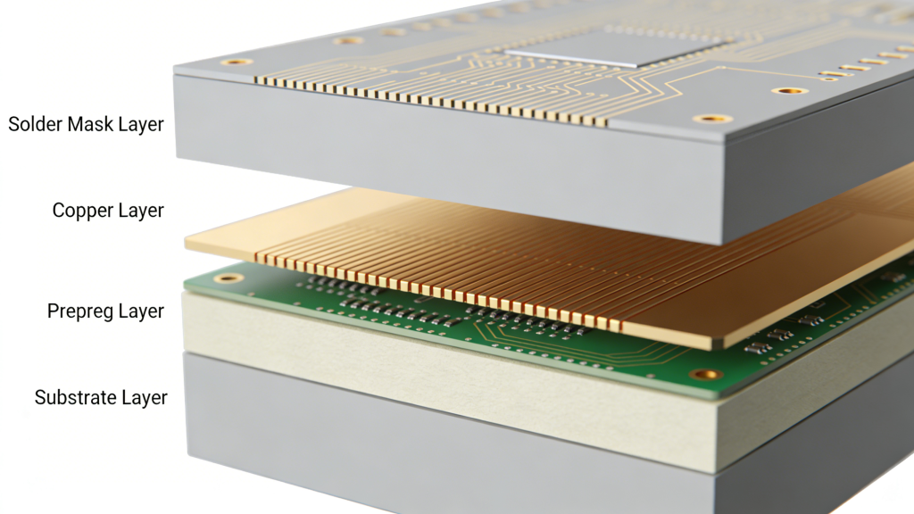
Soldering is a core step in PCBA manufacturing that securely bonds electronic components to printed circuit boards. Wave soldering and reflow soldering are the two dominant industrial processes. Understanding their differences helps you select the ideal method for cost, quality, and assembly type in your PCB production.

What Is Wave Soldering?

Wave soldering is a through‑hole focused assembly process where a PCB passes over a standing wave of molten solder. The liquid solder forms reliable joints on PTH components and bottom‑mounted parts.

Wave soldering process diagram for PCB assembly

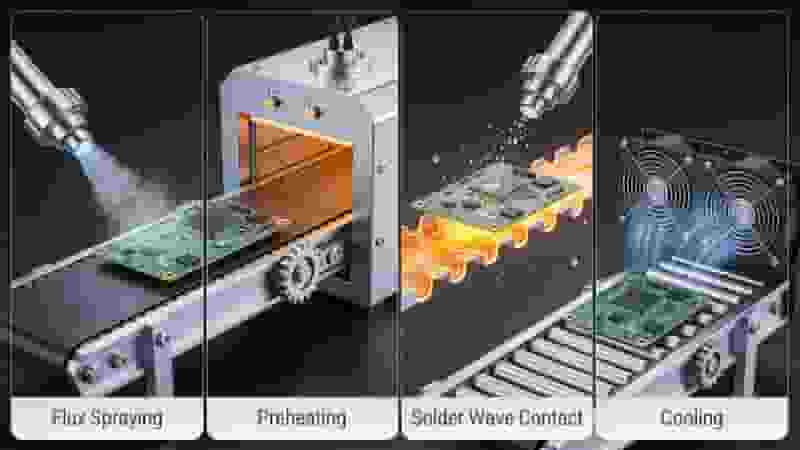
Wave Soldering Process Steps

  1. Flux spraying: cleans surfaces and prevents oxidation
  2. Preheating: stabilizes PCB temperature before soldering
  3. Solder wave contact: forms permanent electrical joints
  4. Cooling: solidifies solder and locks components

Benefits of Wave Soldering

  • Ideal for through‑hole PCB assembly
  • Lower equipment and per‑unit cost for high volume
  • Faster processing than reflow for mixed boards
  • Strong, durable solder joints for industrial use
  • Recirculated solder ensures consistent alloy composition

What Is Reflow Soldering?

Reflow soldering uses solder paste applied via a stencils. Components are placed by pick‑and‑place equipment, then heated in an oven to melt the paste and form permanent bonds. It is the standard for SMT PCB assembly.

Reflow soldering oven and temperature profile for SMT PCB

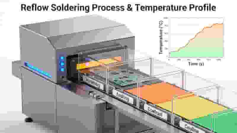
Reflow Soldering Process Steps

  1. Solder paste printing via precision stencil
  2. Component placement (SMDs / chip components)
  3. Preheat and thermal soak to activate flux
  4. Reflow zone melts solder to form joints
  5. Cooling solidifies connections

Advantages of Reflow Soldering

  • Perfect for high‑density SMT assembly
  • Excellent solder joint consistency and quality
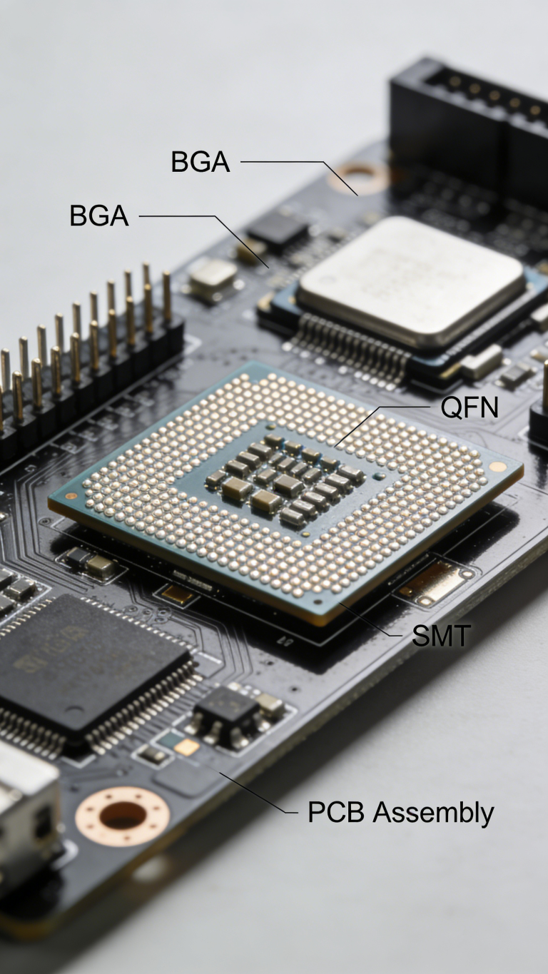
  • Supports ultra‑small components (0402, 0201, BGA)
  • Low risk of bridging or cold joints
  • Process is highly repeatable and automated

Reflow Soldering vs. Wave Soldering: Full Comparison
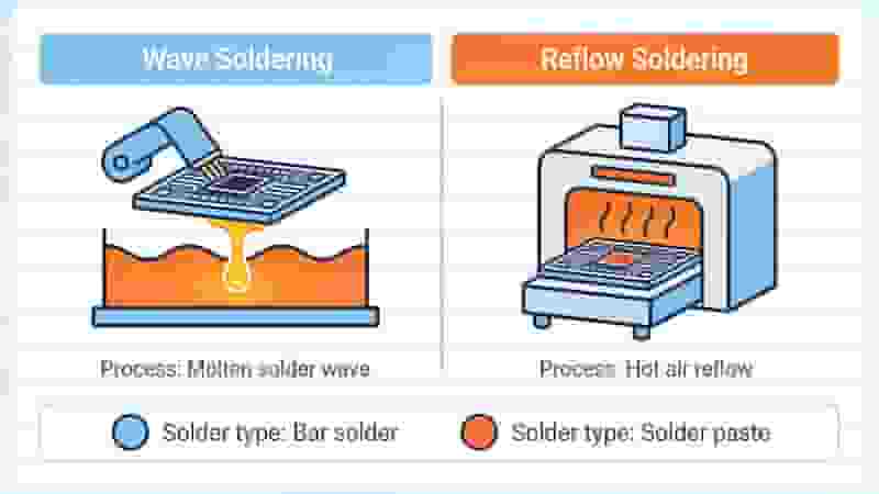
Reflow vs wave soldering comparison for PCB assembly
ItemWave SolderingReflow Soldering
Best ForThrough‑hole (PTH), bottom‑side partsSMT, high‑density, fine‑pitch components
Solder MaterialMolten solder barSolder paste (powder + flux)
Process ComplexityModerate; requires wave tuningControlled via oven profile
CostLower machine costHigher investment; stencil needed
Defect RateHigher for fine componentsVery low for SMT

Which Soldering Method Should You Choose?

Choose wave soldering if you need:

  • Mostly through‑hole components
  • Cost‑sensitive high‑volume production
  • Simple, low‑density PCB assemblies

Choose reflow soldering if you need:

  • Surface‑mount (SMT) or high‑density boards
  • Fine‑pitch chips, BGAs, QFNs
  • Consistent, high‑reliability PCB assembly

Many modern PCBs use both processes: reflow for SMT on top, then wave for through‑hole on bottom.

SMT and through-hole PCB assembly process

Conclusion

Wave soldering remains essential for through‑hole and cost‑focused builds, while reflow soldering dominates modern SMT PCB assembly for precision, density, and reliability. The best choice depends on component types, volume, quality needs, and budget.

We provide professional guidance to select the optimal soldering process for your project.

Need Professional PCB Assembly Service?

We offer full PCB assembly, SMT, through‑hole, reflow, and wave soldering for prototypes to mass production.

Request a Quote Now

Double Sided PCB Structure and Layer Design

Double Sided PCB Manufacturing: Process, Specifications & Custom Solutions 

Posted on
0 Comments
We provide professional Double Sided  PCB manufacturer in China for global industrial buyers, engineers, and procurement teams. Our full capabilities cover prototyping, mass production, DFM, assembly, and strict quality control to meet IPC standards for reliable, high-performance double-layer PCBs.  Why Choose Us for Double Sided PCB Manufacturing  We are a professional manufacturer focused on Double…
4 Layer and 6 Layer Multilayer Flex PCB Stack Up Design

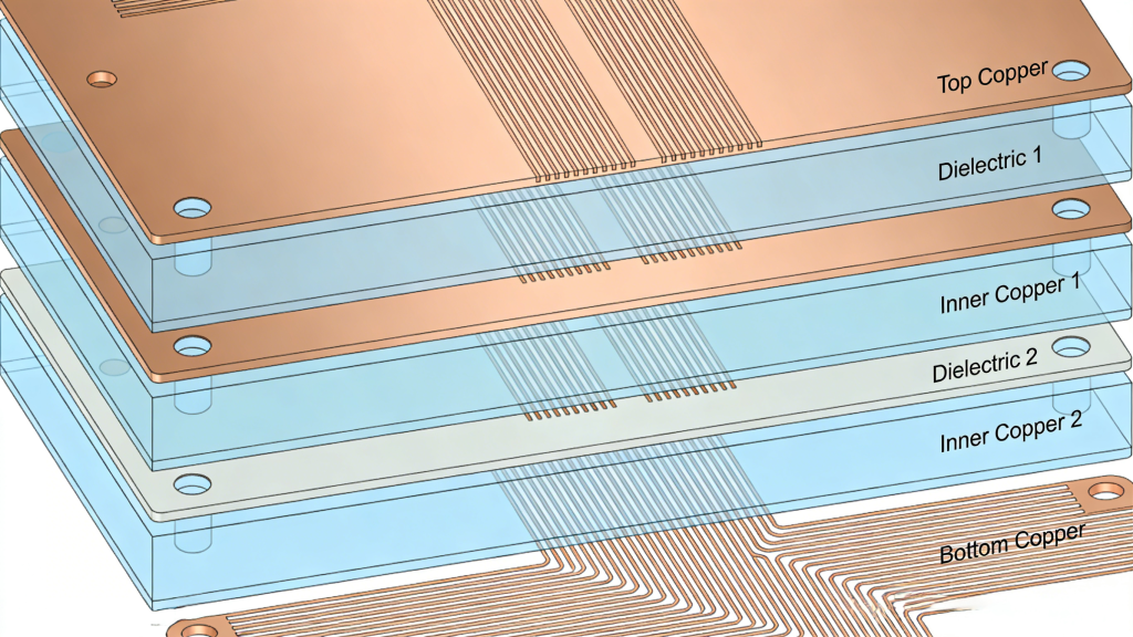
Multilayer Flexible PCB Manufacturer | Custom 4–16 Layer Flex Circuits

Posted on
0 Comments
Lightweight, high‑density multilayer flexible PCB for compact, reliable electronics in consumer, automotive, medical, and industrial applications. Up to 16‑layer flex and rigid‑flex PCB manufacturing with tight tolerances and controlled impedance. 10+ years flex PCB experience in China 1,000,000+ flex circuits shipped per year Quick‑turn prototypes & volume production for multilayer flexible PCB Multilayer Flex PCB…
HDI PCB manufacturing capabilities and technical specifications

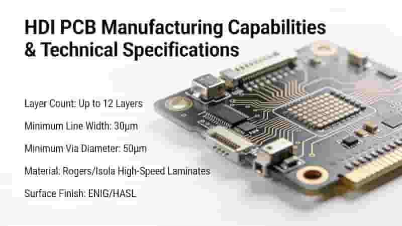
HDI PCB Manufacturing – Microvia, Blind & Buried Via HDI Boards up to 30 Layers

Posted on
0 Comments
We provide professional HDI PCB manufacturing with laser‑drilled microvias, blind vias, buried vias, and advanced stack‑ups for high‑performance, compact electronic devices. Our services include fast prototyping, controlled impedance, strict quality control, and full DFM engineering support. What Is an HDI PCB and Why Choose It? High‑density interconnect (HDI PCB) offers significantly higher wiring density than…
Advanced PCB via technologies including backdrilled, filled, and via-in-pad

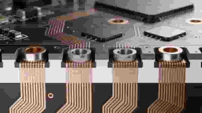
PCB Vias: Complete Guide to Types, Design, Reliability & Applications

Posted on
0 Comments
PCB vias are essential vertical interconnects that enable layer transitions in multilayer printed circuit boards. This professional guide covers via definitions, core types, manufacturing processes, reliability factors, advanced structures, and best practices for engineers and global buyers. What Are PCB Vias A PCB via is a plated vertical electrical connection that routes signals, power, and…
Copper Clad Laminate PCB Raw Material FR4 High Tg

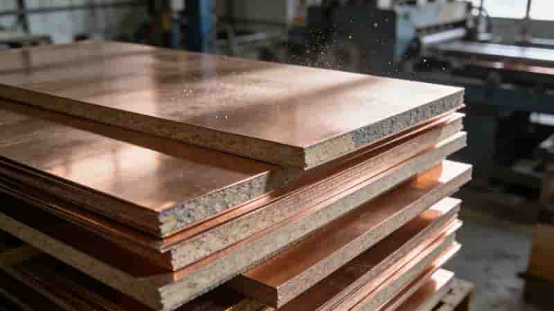
PCB Manufacturing Process Part 1: MI, Cutting & Drilling – Complete Industrial Guide

Posted on
0 Comments
This professional guide covers the core initial stages of PCB manufacturing: Manufacturing Instruction (MI), material cutting, and precision drilling. Learn how industrial processes ensure accuracy, stability, and quality for reliable printed circuit boards. Manufacturing Instruction (MI) The Manufacturing Instruction (MI) is the most critical engineering document in PCB production. It converts Gerber and ODB++ files…
PCB Layer Count Structure Thickness Diagram

Standard PCB Thickness: Complete Guide for Engineers & Buyers

Posted on
0 Comments
Standard PCB thickness is critical for mechanical strength, signal integrity, and assembly compatibility. This guide covers definitions, industry standards, influencing factors, manufacturing constraints, and design best practices for global industrial buyers. What Is Standard PCB Thickness The global standard PCB thickness is 1.57 mm (0.062 in), commonly referenced as 1.6 mm for simplicity. This is…

FAQs About Wave Soldering vs Reflow Soldering

A: Wave soldering lets PCBs pass over molten solder waves, mainly applied to through-hole component assembly. It features low cost and high efficiency for mass production.

A: Reflow soldering melts pre-applied solder paste in an oven, which is the standard process for high-density SMT assembly and tiny components like BGA.

A: Wave soldering uses molten solder for through-hole parts with lower equipment cost; reflow soldering uses solder paste for SMT, delivering better joint quality and lower defect rate.

A: Choose wave soldering for through-hole boards and cost-sensitive mass production; pick reflow soldering for SMT, fine-pitch components and high-reliability requirements.

A: Yes. Many mixed-assembly PCBs adopt reflow soldering for top-side SMT components and wave soldering for bottom through-hole parts.

A: It supports ultra-small and fine-pitch components, ensures uniform solder joints, and effectively reduces bridging and cold solder joint defects.

Similar Posts