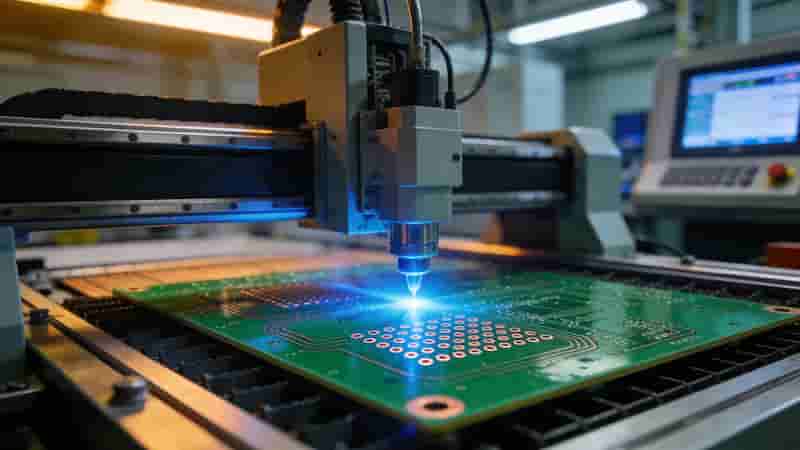
Microvias are core interconnect structures that drive PCB miniaturization and high‑density design. This professional guide covers definitions, types, fabrication, reliability, applications and how we deliver high‑quality microvia PCB solutions for global industrial buyers.
What Are Microvias in PCBs
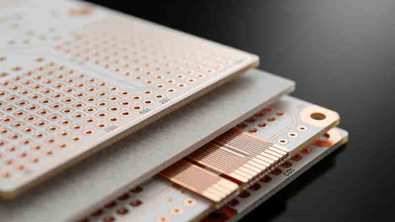
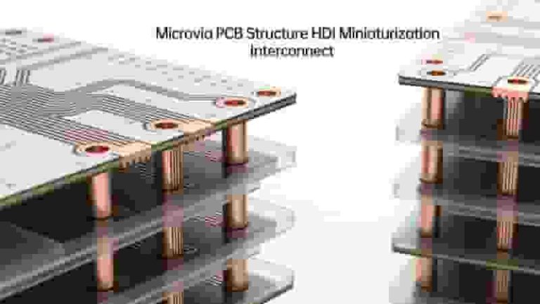
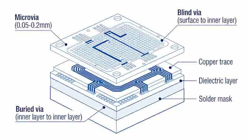
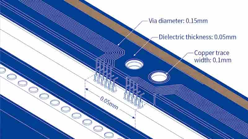
As printed circuit boards integrate more components into smaller spaces, microvias become essential for advanced PCB miniaturization. A microvia is a tiny vertical interconnect used in high‑density PCB designs, typically 0.005–0.015 inches (0.13–0.38mm) in diameter.
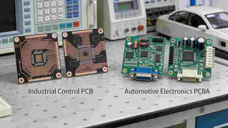
Compared with traditional through‑hole vias, microvias reduce board thickness and layer count while preserving electrical performance. They enable higher routing density and smaller form factors for smartphones, wearables, automotive controllers and medical devices.
Types of Microvias
There are two mainstream processes for manufacturing microvias in PCB production: laser drilling and photoimageable technology.
Laser‑Drilled Microvias
Laser systems (CO₂, YAG, excimer) create precision microvias down to 0.005 inches. They support high depth‑to‑diameter ratios and fine capture pads, ideal for high‑density PCB designs.
- High precision and small via annular rings
- Depth‑to‑diameter ratio up to 15:1
- Suitable for high‑layer‑count PCB
Photoimageable Microvias
UV patterning and copper plating form microvias at lower cost for moderate‑density boards. They support large production panels but have larger minimum feature sizes.
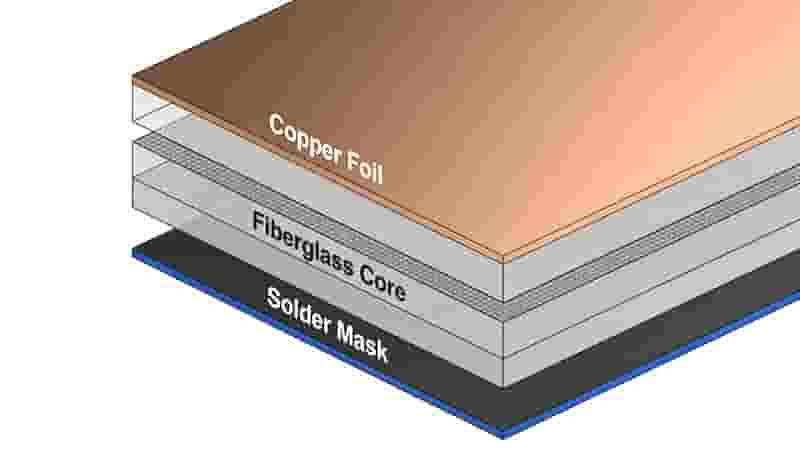
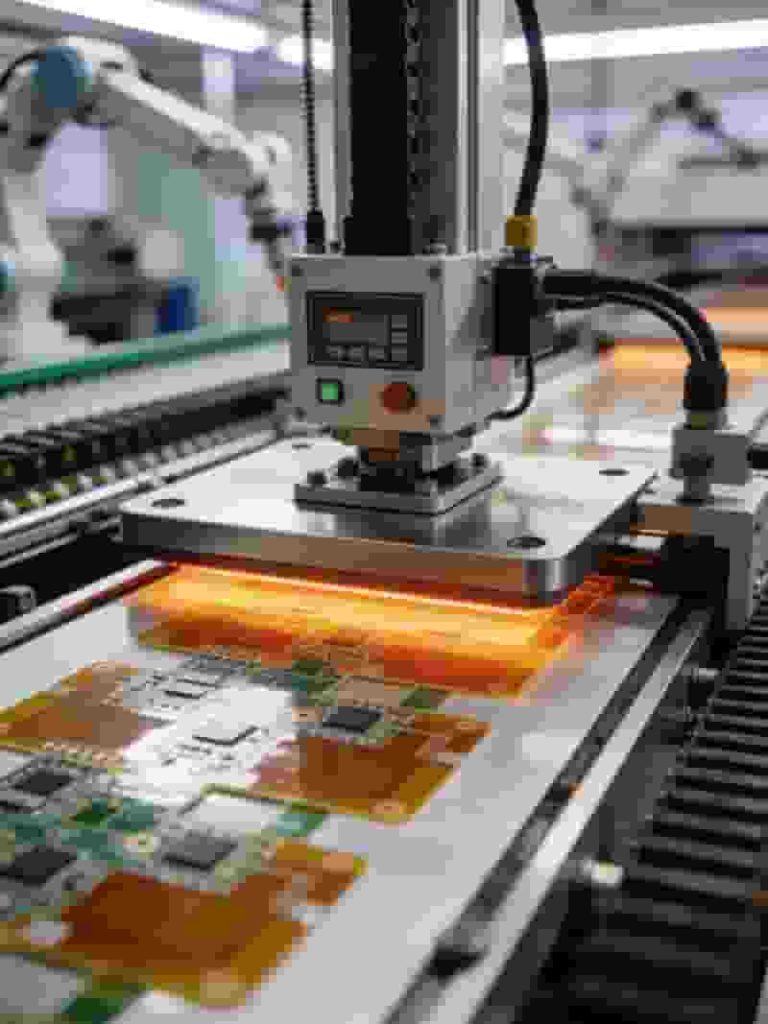
Microvia PCB Technology & Fabrication
Reliable microvia PCB production requires strict control of stacking, drilling, metallization and quality assurance.
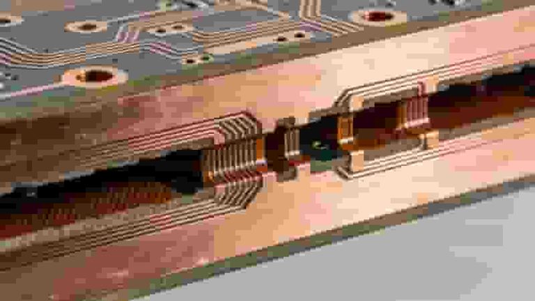
Stacked & Staggered Microvias
Stacked microvias align vertically to save space; staggered microvias offset positions to lower thermal stress and improve reliability.
Plating & Quality Control
Electroless copper and electroplating ensure void‑free filling inside microvias. Statistical process control maintains consistent diameter, depth and plating quality.
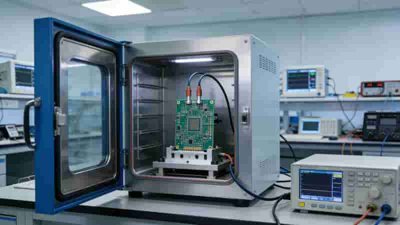
Microvia Reliability Factors
Microvia durability depends on thermal cycling, pad design, materials and assembly protection.
- CTE mismatch between copper and laminate
- Optimized capture pad size for microvias
- Underfill and encapsulation to improve stability
Industry Applications of Microvia PCBs
Microvia PCBs are widely used in industries demanding miniaturization and high performance:
- Consumer Electronics: smartphones, tablets, wearables
- Automotive: ADAS, infotainment, power control
- Aerospace & Defense: guidance systems, high‑reliability modules
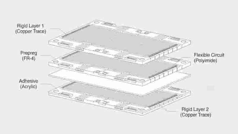
- Medical Devices: implants, diagnostic equipment, rigid‑flex PCB
The Future of Microvias in PCB Design
Advances in laser drilling and plating will enable smaller microvias with higher aspect ratios. Microvia technology will continue supporting 6–12+ layer HDI boards, AI hardware and high‑speed computing applications.
Our Microvia PCB Manufacturing Capabilities
We specialize in high‑precision microvia PCB design, prototyping and mass production for global buyers. Our advanced laser drilling systems, strict quality inspection and engineering expertise ensure stable performance and competitive costs.
- Advanced laser drilling for microvias down to 0.13mm
- Stacked / staggered microvia design support
- 100% AOI and electrical testing for reliability
- Fast prototypes and volume export production
Summary
Microvias are foundational to PCB miniaturization and high‑density interconnect design. They deliver smaller size, higher performance and greater reliability for modern electronics. As a professional PCB manufacturer, we provide customized microvia PCB solutions to meet your engineering and commercial requirements.
Get Your Microvia PCB Quote Today
Contact us for custom design, prototype and mass production of high‑quality microvia PCBs.
Inquire Now | Custom Quote
Aluminum PCB vs FR4 PCB: Full Technical Comparison for Industrial & Export Buyers
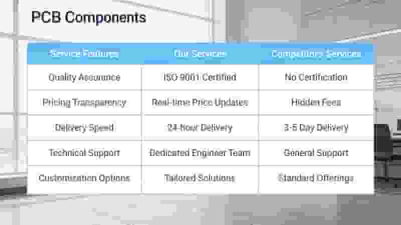
PCB Components Purchasing Services | Global Electronic Components SourcingPCB
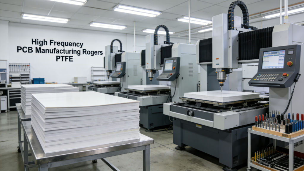
High Frequency PCB Manufacturer & RF PCB Fabrication
What Is the Difference Between PCB and PCBA? A Complete Guide for Industrial Buyers
Flexible PCB Coverlay: What It Is & How It Works