Custom PCB costs in 2025 are shaped by material selection, layer count, board dimensions, manufacturing processes, surface finish, order volume, tolerances, certifications, and global supply chains. This professional guide breaks down all cost drivers with technical details, comparison tables, and actionable cost‑saving strategies for industrial buyers, engineers, and importers.
PCB Base Material & Cost Impact
The substrate is one of the biggest drivers of custom PCB costs. Standard FR‑4 delivers the best value for most applications, while high‑frequency or high‑thermal materials add significant cost.
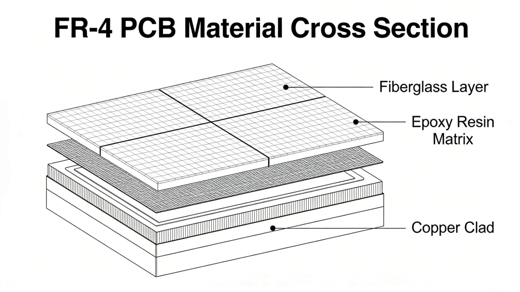
FR‑4 (glass‑reinforced epoxy laminate) is the default for consumer, industrial, and IoT electronics. High‑performance substrates such as Rogers, aluminum, ceramic, or polyimide cost 3–15 times more due to material purity and specialized processing.
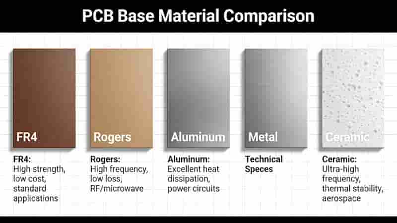
In 2025, global material prices and supply stability further affect custom PCB costs. Standard FR‑4 remains stable, while high‑frequency substrates see 5–15% volatility.
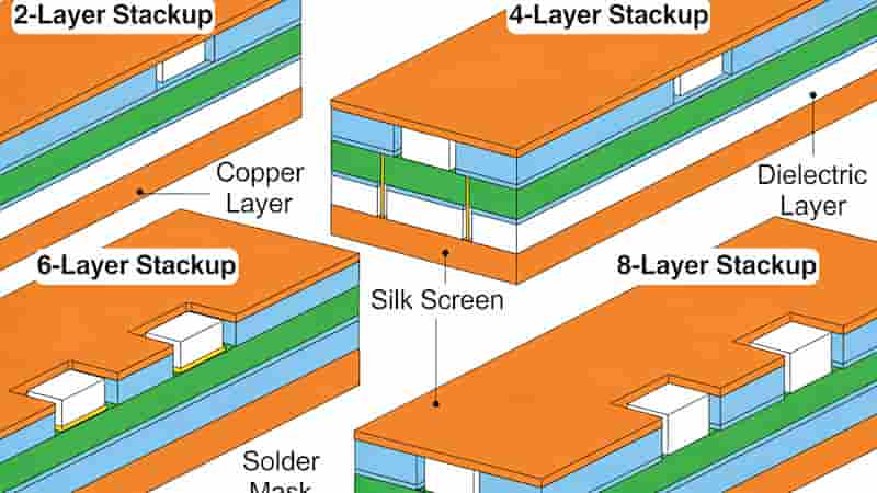
Layer Count & Stackup Complexity
Each additional layer directly raises custom PCB costs by increasing lamination, drilling, alignment, and inspection steps.
2-layer boards are the most economical. 4-layer boards support better signal integrity and density. 6-layer and above are used for high‑speed, industrial, automotive, and medical designs. Each extra layer typically adds 20–30% to manufacturing cost.
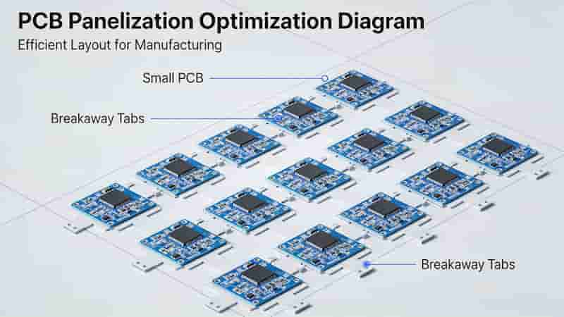
Board Size & Panel Utilization
Larger board area increases raw material usage and handling cost, directly lifting custom PCB costs. Optimized dimensions and panelization reduce waste and per‑unit price.
Most manufacturers price by usable area. Irregular shapes, oversized boards (>500 sq.cm), and low panel yield lead to surcharges. Standard rectangular designs minimize cost.
Manufacturing Processes & Tolerances
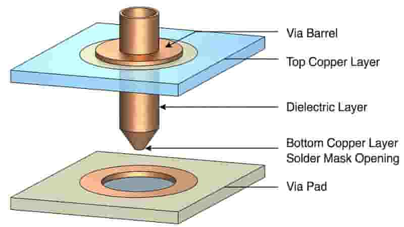
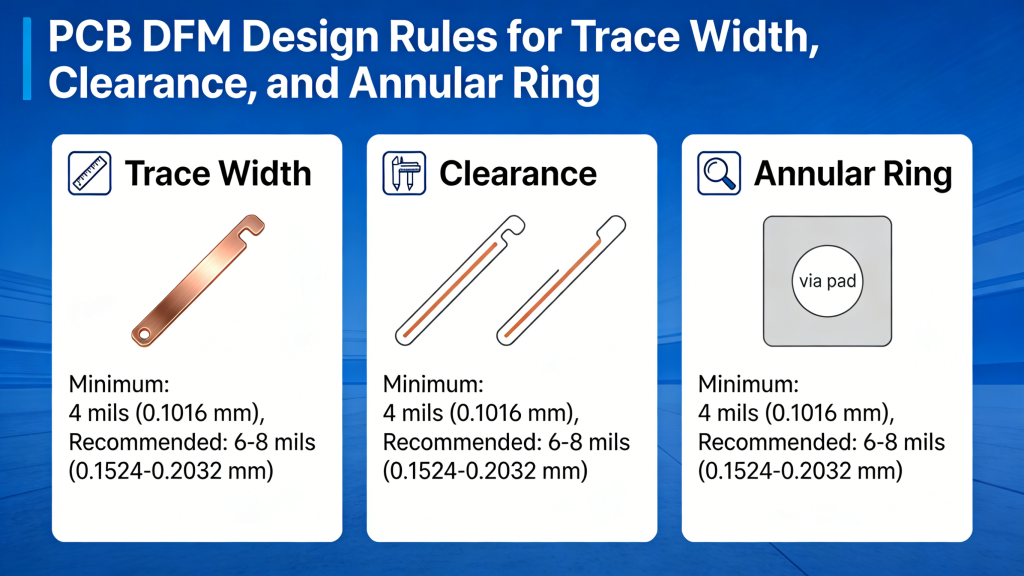
Fine lines, tight spacing, microvias, controlled impedance, heavy copper, and HDI structure all increase custom PCB costs because they require advanced equipment and stricter quality control.
Standard tolerances (≥6 mil trace/space) are cost‑effective. Finer features (4 mil or below) add 20–60% cost. HDI with laser‑drilled microvias is used only for compact, high‑density products.
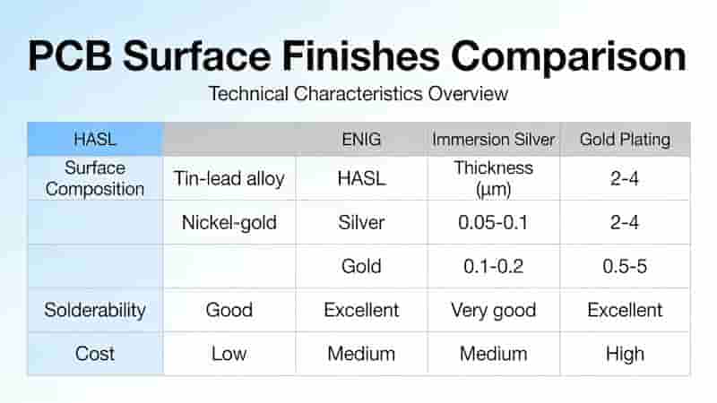
Surface Finish Selection
Surface finish affects solderability, shelf life, reliability, and custom PCB costs. HASL is the most economical; ENIG, ENEPIG, and immersion silver are premium options.
Lead‑free HASL is standard for cost‑sensitive projects. ENIG provides flat bonding for fine‑pitch components but increases cost significantly. Gold plating is used for high‑wear connectors.
Order Volume & Lead Time
Economies of scale strongly influence custom PCB costs. Prototypes have high setup cost per unit; mass production spreads tooling and labor across thousands of units.
Rush lead times (2–3 days) add 20–50% cost. Standard lead times (7–10 days) allow optimized production scheduling and lower pricing.
Testing & Certifications
Testing and certifications ensure reliability but raise custom PCB costs. AOI, E‑test, flying probe, X‑ray, thermal cycling, and compliance (UL, IPC, RoHS) all add expense.
Basic testing is included in standard orders. Advanced inspection and regulatory certifications are required for automotive, medical, aerospace, and industrial applications.
Cost Factor Comparison Table
| Factor | Cost Impact | Typical Range | Cost‑Saving Tip |
|---|---|---|---|
| Base Material | Very High | FR‑4: Low; Rogers: High | Use FR‑4 unless high frequency is required |
| Layer Count | High | 2L < 4L < 6L < 8L+ | Minimize layers with smart routing |
| Board Size | Medium | Larger = higher cost | Optimize dimensions; use panelization |
| Surface Finish | Medium | HASL < ENIG < Gold | Choose HASL for standard projects |
| Volume | Very High | Prototype > Bulk | Order in bulk to reduce unit cost |
2025 PCB Cost Trends
1. Global material price stability for standard FR‑4, with mild increases for high‑performance substrates.
2. Automation lowers labor cost and improves consistency, reducing custom PCB costs for mass production.
3. Green and halogen‑free materials gain adoption with a small cost premium.
4. HDI and high‑speed PCB demand grows, supporting premium pricing for advanced manufacturing.
Proven Cost‑Saving Strategies
• Use standard FR‑4 and avoid specialty materials unless necessary
• Reduce layer count through optimized routing
• Relax trace/space tolerances to ≥6 mil where possible
• Choose standard lead time to avoid rush fees
• Panelize multiple designs to share setup cost
• Use lead‑free HASL for non‑critical applications
• Plan order volume to leverage economies of scale
Summary
Understanding custom PCB costs in 2025 means balancing material, layer count, size, processes, finish, volume, and quality requirements. By making informed design and sourcing decisions, you can reduce total cost by 20–50% while maintaining performance and reliability.
For industrial buyers, importers, and engineering teams, transparent cost breakdowns and professional manufacturing support are key to stable budgeting and scalable production.
Inquiry & Custom Quote
Do you need an accurate, detailed quote for your custom PCB project? Send us your Gerber files, layer count, quantity, material, surface finish, and target lead time.
We provide professional PCB manufacturing with competitive pricing, strict quality control, and reliable global delivery for industrial, medical, automotive, IoT, and consumer electronics.
Contact us today for your free official quotation and DFM review.
Request Your Custom PCB Quote Now
Professional, cost‑effective PCB solutions for global buyers
What Are Tented Vias? A Complete PCB Design Guide
PCB Immersion Gold (ENIG) Surface Finish: Benefits, Process & Full Guide
Design for Manufacturability and Assemblability of Printed Circuit Board
Through-hole PCB Assembly Service | IPC Certified THT PCBA Solutions
Why Choose FR-4 PCBs in 2025? Benefits, Applications & Custom Solutions for 5G, IoT & EVs