Learn how to build multilaye multilayer PCB stack-upr PCBs with this complete guide covering stack‑up design, step‑by‑step manufacturing, IPC standards, material selection, and long‑term storage to ensure high‑reliability circuit boards for industrial, medical, automotive, and telecom applications.
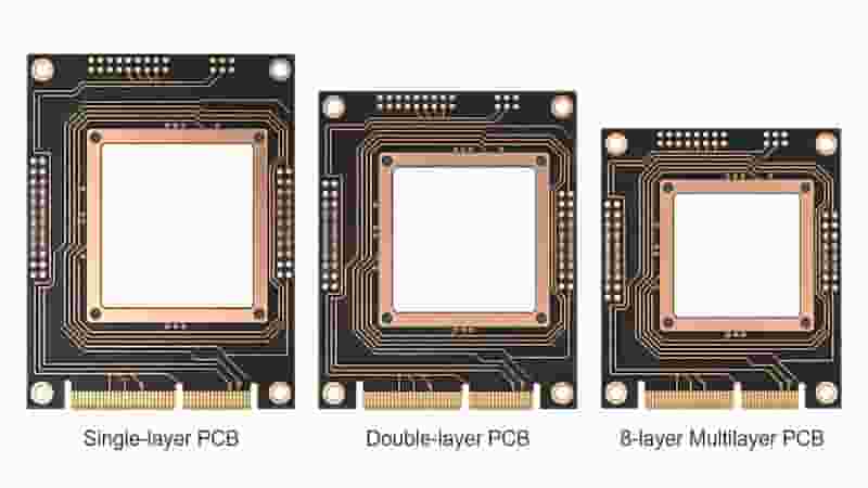
What Is a Multilayer PCB?
A multilayer PCB integrates three or more conductive copper layers bonded with insulating core and prepreg materials, typically ranging from 4 to 50+ layers for high‑density electronics. Compared to single or double‑sided PCBs, multilayer PCB designs deliver higher routing density, better signal integrity, stable power distribution, and stronger anti‑interference performance, making them essential for smartphones, servers, medical devices, automotive electronics, and avionics systems.
Key Core Terms
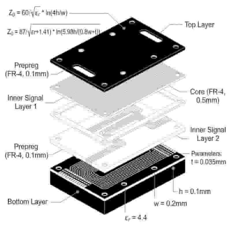
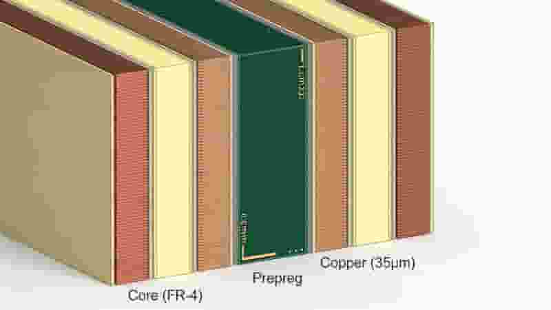
- Core: Rigid dielectric substrate (commonly FR‑4) clad with copper on both sides, forming inner conductive layers.
- Prepreg: Semi‑cured epoxy resin glass cloth, used to insulate and bond layers during high‑temperature lamination.
- Surface Layers: Top and bottom outer layers for component mounting, soldering, and external signal connection.
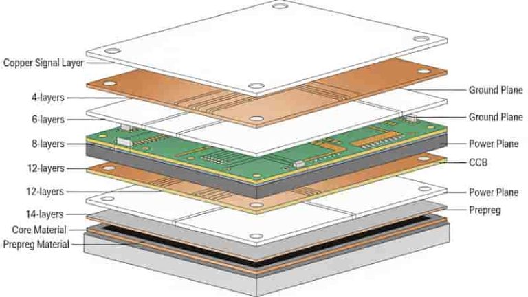
Multilayer PCB Stack‑Up Design & Layer Configurations
Stack‑up directly determines the electrical performance, thermal management, and structural stability of a multilayer PCB. Symmetric layer arrangement is strongly recommended to avoid warpage; even layer counts (4, 6, 8, 10, 12) are industry standard.
4‑Layer Multilayer PCB Stack‑Up
The most cost‑effective multilayer PCB structure, ideal for consumer electronics and smart home devices.
- Layer 1: Top Signal
- Layer 2: GND Plane
- Layer 3: Power Plane
- Layer 4: Bottom Signal
- Standard thickness: 1.6 ± 0.16 mm
6‑Layer Multilayer PCB Stack‑Up
Suitable for industrial controls and automotive sensors. Inner layers are dedicated to GND and power to reduce EMI and crosstalk.
- Typical thickness: 1.6–2.0 mm
- Supports moderate‑complexity signal routing and stable power delivery
8‑Layer & Higher Multilayer PCB Stack‑Up
Designed for high‑speed telecom, medical imaging, and aerospace equipment. Multiple cores and prepreg layers ensure excellent signal integrity and thermal control.
- 8‑layer: 2.4 ± 0.24 mm
- 12‑layer: 2.8–3.2 mm
- Supports blind vias, buried vias, and HDI design
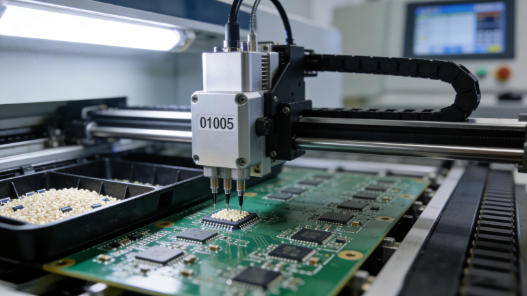
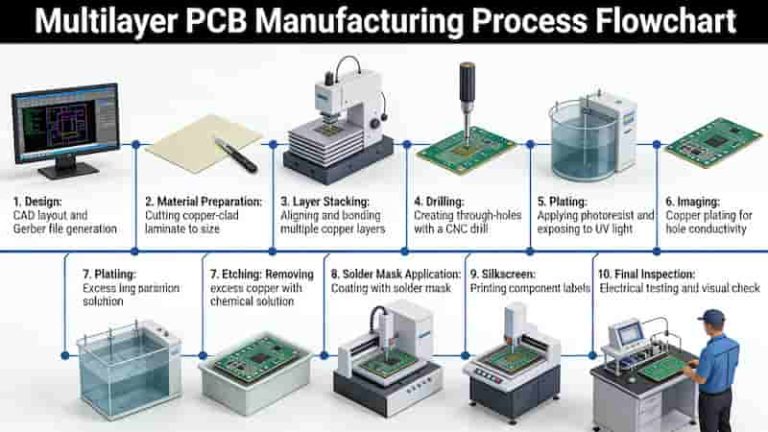
Multilayer PCB Full Manufacturing Process
Producing a reliable multilayer PCB requires precision processing and closed‑loop quality control.
1. Material Preparation
Select high‑speed FR‑4, Rogers, or other high‑frequency materials based on application needs. Inner cores are pre‑treated for reliable bonding.
2. Layer Stacking & Alignment
Copper foils, prepreg, and inner cores are stacked in fixed order and precisely aligned with positioning pins to avoid layer shift.
3. High‑Temperature Lamination
Heat and pressure cure the prepreg, permanently bonding all layers into a solid multilayer PCB core panel.
4. Drilling, Plating & Etching
CNC drilling, electroless copper plating, pattern transfer, and etching form conductive paths and interlayer connections.
5. Surface Finish & Testing
Apply HASL, ENIG, immersion silver, or other finishes. Complete electrical testing, impedance testing, and AOI optical inspection.
IPC Standards for Multilayer PCB
Compliance with IPC standards ensures global market acceptance and long‑term performance of your multilayer PCB.
- IPC‑4101E: Base material specification for rigid multilayer PCB
- IPC‑ML‑960: Qualification for mass lamination panels
- IPC‑6012: Performance specification for rigid printed boards
- IPC‑A‑600: Acceptability criteria for printed boards
Multilayer PCB Storage Guidelines
To preserve solderability and reliability:
- Use vacuum‑sealed packaging with desiccant
- Store in dry, temperature‑controlled environment (18–25°C, RH < 60%)
- Avoid direct sunlight, moisture, and mechanical stress
Conclusion
Building a high‑performance multilayer PCB depends on rational stack‑up design, standardized manufacturing, strict IPC compliance, and proper storage. From 4‑layer prototypes to 50+ layer high‑speed boards, we provide full engineering support and reliable manufacturing for global buyers.
Get Your Multilayer PCB Custom Solution
Contact us for stack‑up design, DFM review, free quotation, and fast lead times for industrial & export‑grade multilayer PCB.
Request a Quote Now

What is a PCB Bill of Materials (BOM) and How to Create One

How to Select the Right Low-volume PCB Assembly Manufacturer
Flexible PCB Cost in 2025: Why It’s Expensive and Proven Ways to Save
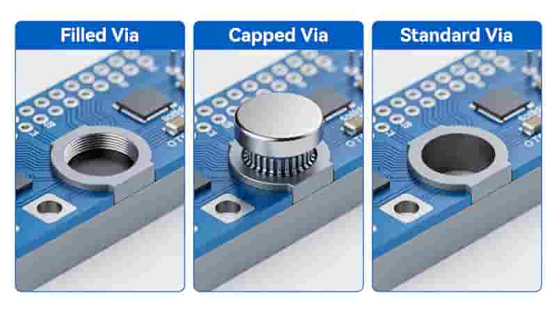
Filled and Capped Vias: Boost PCB Reliability for Industrial & Export Applications
What is FR-4 Material in PCB Fabrication? The Complete Professional Guide