PCB Immersion Gold (ENIG) is a premium lead-free surface finish delivering superior solderability, flatness and oxidation resistance for high-reliability printed circuit boards. This guide explains definition, advantages, limitations, manufacturing steps and comparisons for engineers and global buyers.
What Is PCB Immersion Gold (ENIG) Surface Finish
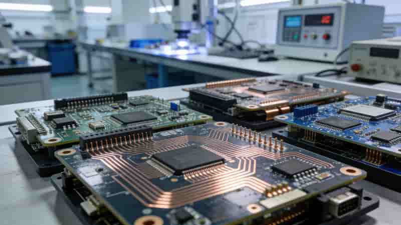
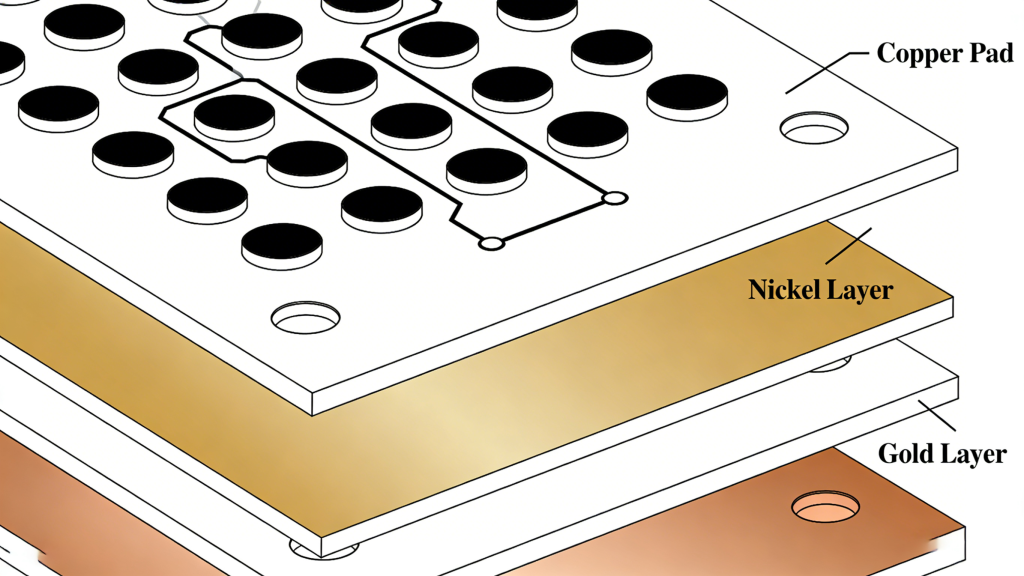
Electroless Nickel Immersion Gold (ENIG) is a widely adopted chemical surface treatment for PCBs. It deposits a nickel-phosphorus alloy layer followed by a thin immersion gold layer without electric current.
This finish protects copper pads, prevents oxidation, ensures stable solderability, and supports high-precision assembly including BGAs, flip chips and fine-pitch SMT components.
Key Benefits of ENIG Surface Finish for PCBs
ENIG provides critical advantages for industrial and high-performance PCB applications:
- Ultra-Flat Surface: Perfect for fine-pitch SMT, BGAs and lead-free assembly
- Excellent Oxidation Resistance: Long shelf life and reliable storage
- Stable Electrical Performance: Consistent signal integrity and connectivity
- High Temperature Resistance: Withstands multiple reflow cycles
- Lead-Free & RoHS Compliant: Safe for global markets
- Strong PTH Performance: Reliable protection for plated through-holes

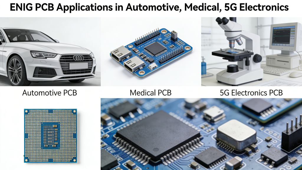
Applications of ENIG Surface Finish
ENIG is widely used in high-reliability electronics worldwide:
- Automotive electronics (engine, safety, infotainment)
- Medical devices and diagnostic equipment
- 5G communication, RF and high-frequency circuits
- High-density consumer electronics with BGAs
- Industrial control and aerospace systems
Disadvantages of ENIG Surface Finish
You should consider these limitations when selecting ENIG:
- Higher Cost: More expensive than HASL, OSP due to gold material
- Black Pad Risk: Possible nickel corrosion under poor process control
- Limited Reworkability: Rigid structure complicates repairs
- RF Signal Loss: Nickel layer may impact high-frequency performance
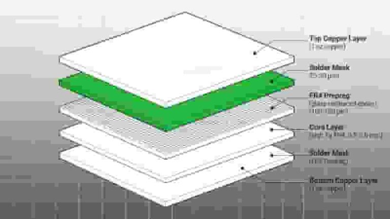
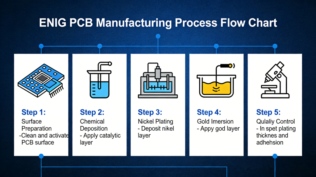
ENIG Manufacturing Process
The ENIG process uses controlled chemical deposition:
- Surface Preparation: Clean, micro-etch and activate copper surfaces
- Electroless Nickel Deposition: Deposit 3-6 μm Ni-P alloy layer
- Immersion Gold: Apply 0.05-0.1 μm thin gold layer
- Cleaning & Drying: Rinse, dry and inspect quality
Standard thickness: Nickel 100-200 μin; Gold 10-15 μin.
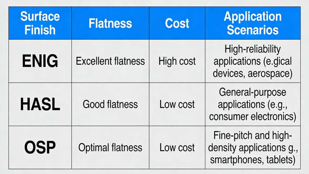
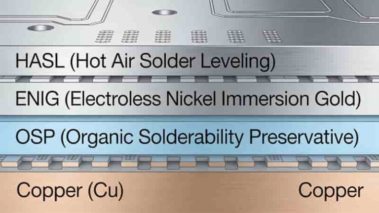
ENIG vs Other PCB Surface Finishes
| Finish | Cost | Flatness | Best For |
|---|---|---|---|
| ENIG | High | Excellent | BGA, SMT, High-Reliability |
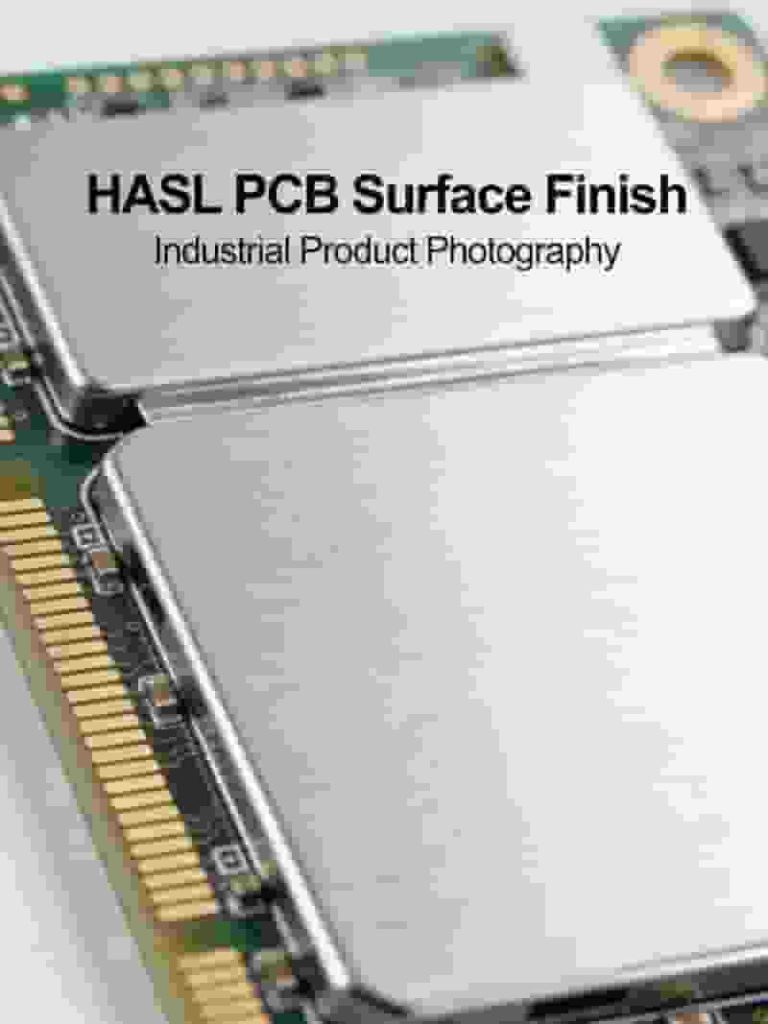
| HASL | Low | Poor | General Purpose |
| OSP | Low | Good | High Volume, Short Shelf Life |
| ENEPIG | Very High | Excellent | High-Frequency, Advanced |
Conclusion
PCB Immersion Gold (ENIG) is a top-tier surface finish offering excellent flatness, solderability, oxidation resistance and lead-free compliance. It is the preferred choice for high-precision SMT, BGA and high-reliability PCB applications worldwide.
Understanding ENIG helps engineers and buyers select the optimal finish to improve yield, reliability and product lifecycle.
Inquiry & Custom PCB Quote
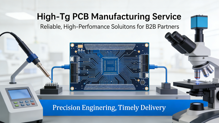
We specialize in high-quality ENIG PCB manufacturing for global industrial clients, with strict IPC standards, reliable process control and competitive pricing.
Contact us today for your custom ENIG PCB solution, prototype or mass production quote:
- Send Gerber files and BOM for free DFM analysis
- Get fast, accurate pricing and lead time
- Customize layer count, thickness and specifications
- 100% quality inspection guaranteed
Request ENIG PCB Quote Now
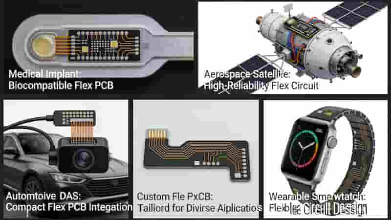
Custom Flex PCB: Tailored Solutions for Your Applications
HDI PCB Manufacturing – Microvia, Blind & Buried Via HDI Boards up to 30 Layers
Heavy Copper PCB Manufacturing & Thick Copper PCB Fabrication Service
High-Precision PCB & SMT Stencil Manufacturing
HASL: Hot Air Solder Leveling for PCB Surface Finish