Master PCB DFM and DFA best practices to streamline manufacturing and assembly. This professional guide covers critical design rules, common errors, and practical solutions for high‑quality, high‑yield PCB production.
Why PCB DFM and DFA Matter
High‑quality PCB starts with optimized design. PCB DFM (Design for Manufacturability) and DFA (Design for Assembly) ensure your board is cost‑effective, reliable, and easy to produce at scale.
PCB DFM aligns design with real fabrication limits. DFA simplifies component placement and soldering for smooth assembly. Bad design causes defects, delays, and higher costs.
These rules work for rigid, flexible, and HDI PCB designs to deliver consistent quality and faster time to market.
What is PCB DFM
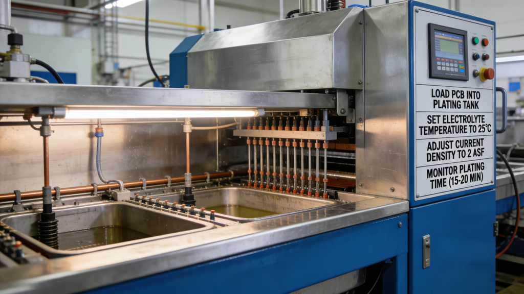
PCB DFM ensures your design matches standard manufacturing processes to reduce defects, lower cost, and speed up production. It optimizes board size, vias, traces, and materials for real‑world fabrication.
Without PCB DFM, even advanced designs can fail due to incomplete vias, solder bridges, or etching failures.
Key PCB DFM Goals
- Reduce manufacturing defects like open circuits and incomplete plating
- Shorten production cycles with simplified fabrication steps
- Lower cost through better material use and higher first‑pass yield
Key PCB DFM Considerations
Board Size and Tolerance
Most factories support up to 500mm × 500mm with ±0.1mm tolerance. Leave 5–10mm process edges for stable handling.
Material and Thickness
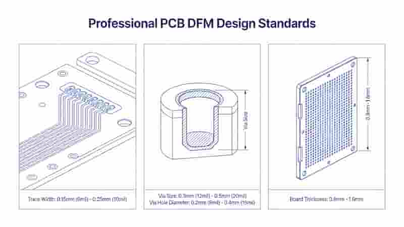
Use standard FR‑4 for rigid PCB, polyimide for flex boards. Typical thickness: 0.8mm to 1.6mm.
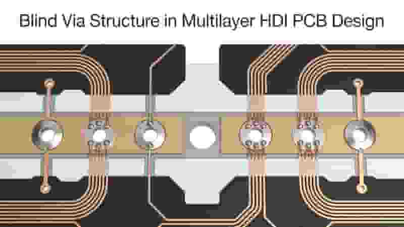
Thickness‑to‑Via Ratio
Ideal ratio is 8:1 (e.g., 1.6mm board with 0.2mm vias) for reliable plating. Higher ratios risk incomplete holes.
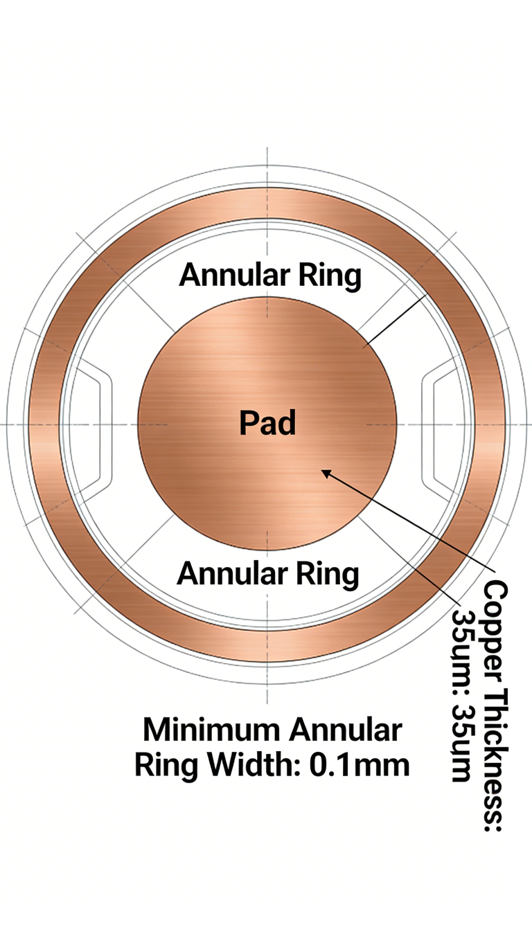
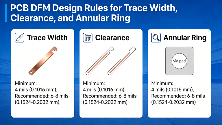
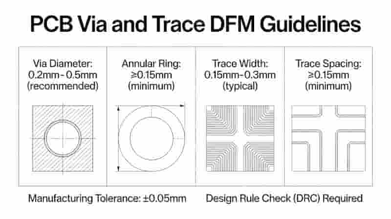
Trace and Land Design
Standard: 0.1mm trace / 0.1mm space. HDI: 0.05mm trace / 0.05mm space. Pads must match component specs.
What is PCB DFA
PCB DFA optimizes layout for fast, error‑free component installation, soldering, and testing. It reduces assembly defects and improves reliability.
Poor DFA causes solder bridges, misalignment, and difficult testing, directly lowering yield and increasing cost.
Key DFA Goals
- Speed up assembly with clear, logical layout
- Ensure strong, reliable solder joints
- Simplify testing, inspection, and rework
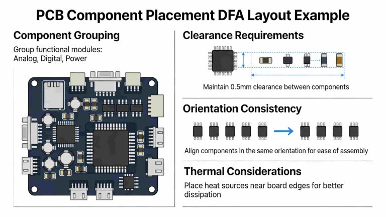
Key PCB DFA Considerations
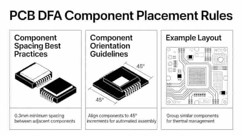
Component Spacing
Manual: 1mm apart. Auto SMT: 0.5mm apart. Keep 5mm clear from board edges.
Pad and Solder Mask
SMT pad: ~1.0mm². Through‑hole pad: ~2.0mm². Solder mask prevents bridges and improves quality.
Thermal Management
Place heat‑generating parts with enough clearance and cooling paths to avoid overheating.
Test Points and Markings
Put test points in accessible areas. Use clear polarity marks to avoid assembly errors.
PCB DFM vs DFA Comparison
| Item | PCB DFM | PCB DFA |
|---|---|---|
| Focus | Fabrication capability | Assembly efficiency |
| Main Factors | Traces, vias, materials, tolerances | Components, pads, spacing, test points |
| Purpose | Reduce production failures | Lower assembly defects |
| Benefit | Lower fabrication cost | Faster assembly & higher yield |
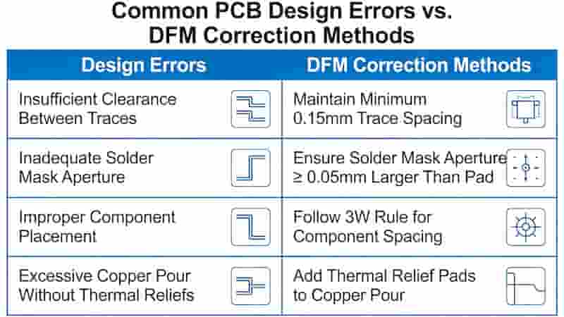
Common PCB Design Mistakes
- Ignoring factory capabilities: Using ultra‑fine features without confirmation
- Insufficient spacing: Crowded parts cause solder bridges and rework
- Bad via design: Tiny vias or extreme ratios cause plating failure
- No solder mask: Increases short‑circuit risk in mass production
- Poor EMC design: Bad routing creates signal interference
Conclusion
Following PCB DFM and DFA best practices is essential for building high‑quality, low‑cost PCB with minimal defects and fast production.
By optimizing traces, vias, spacing, and materials, you eliminate common design errors and prepare your boards for mass production.
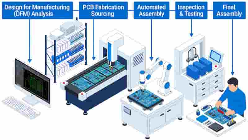
We provide full PCB manufacturing and assembly with strict DFM/DFA compliance to support industrial buyers worldwide.
Get Professional PCB DFM & DFA Support
Request a free PCB DFM review, custom quote, or expert design consultation. We offer fast lead times, reliable quality, and full turnkey services.
Free DFM Check
Get a Quote
SMT vs SMD: What’s the Difference in PCB Assembly?
Affordable PCB Prototypes & Assembly Services
How to Choose a Reliable PCB Prototype Manufacturer for Electronics Projects
SMT PCB Assembly Services for Prototypes & Production
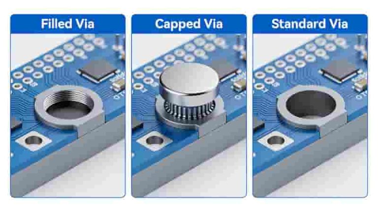
Blind Vias & Buried Vias in PCBs – The Complete Engineering Guide