We provide professional single layer PCB manufacturing and cost-effective single sided PCBs for LED lighting, power supplies, consumer electronics, and industrial equipment. Our ISO & IPC‑certified production ensures stable quality, fast lead times, and free DFM analysis for prototypes and mass production.
Single-Layer PCB Definition
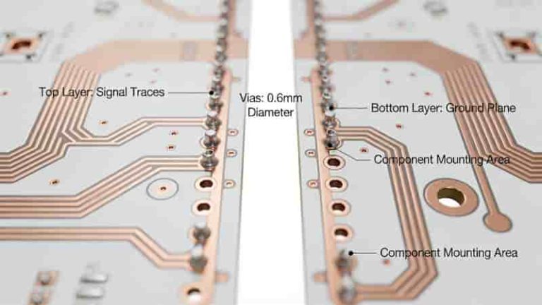
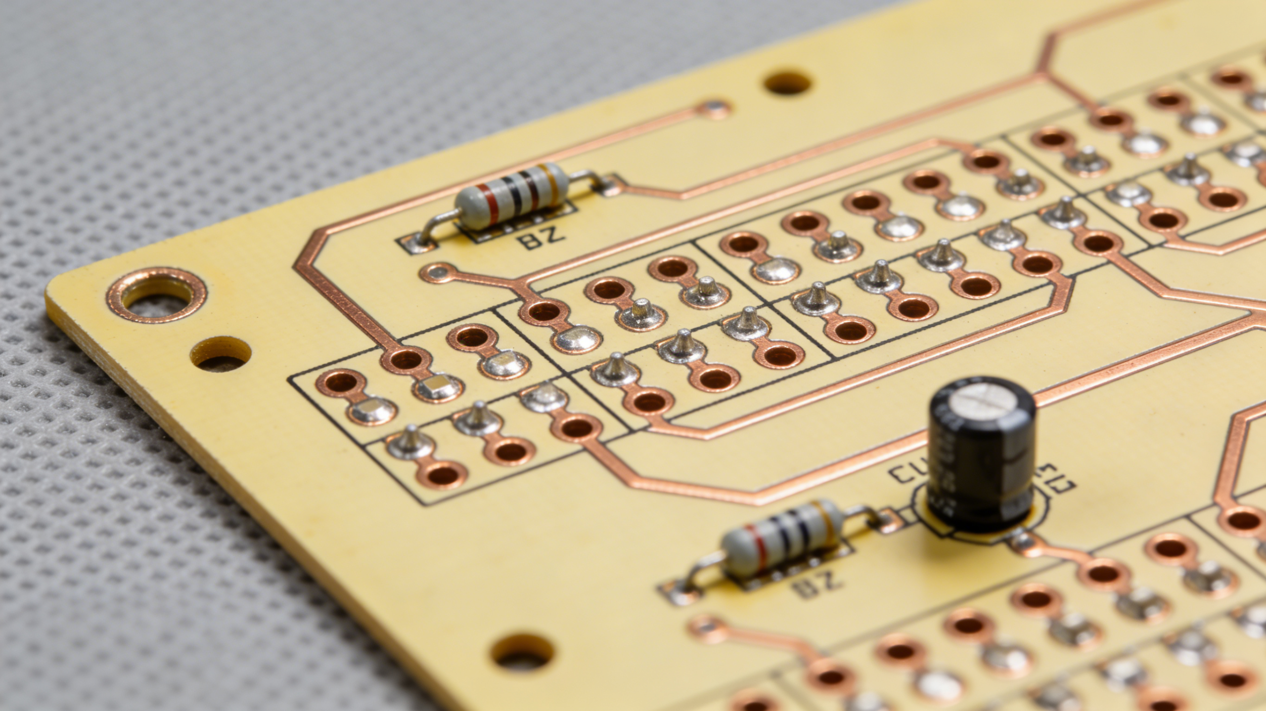
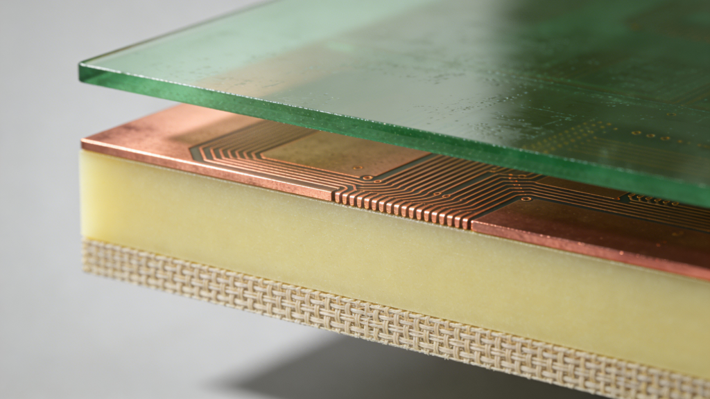
A single layer PCB (also called single sided PCB) has only one conductive copper layer bonded to a dielectric substrate such as FR‑4, aluminum, or flexible materials. It is coated with solder mask and marked with silkscreen for component identification. This simple structure makes it the most cost‑effective solution for basic electronic circuits.
Types of Single Layer PCBs
Single Layer Rigid PCB
Built on FR‑4 material, widely used in calculators, remote controls, and low‑power electronics. Our single layer PCB manufacturing ensures stable performance and low cost.
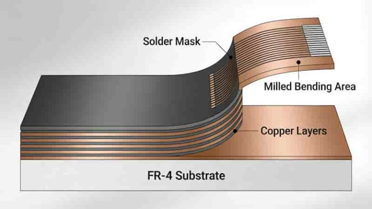
Single Layer Flexible PCB
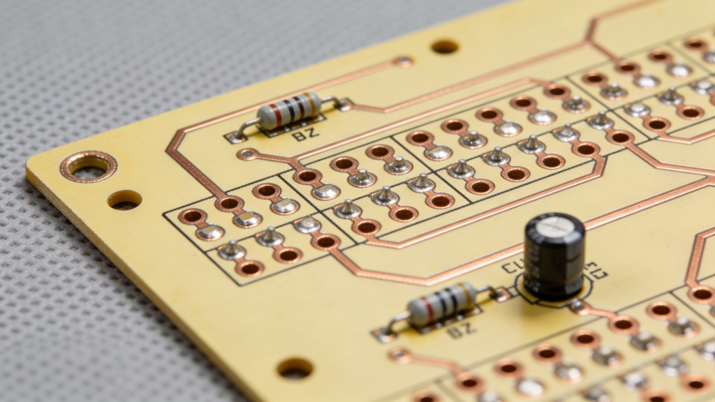
Made of polyimide film for wearable devices, medical sensors, and compact assemblies. We deliver high‑precision flexible single sided PCBs.
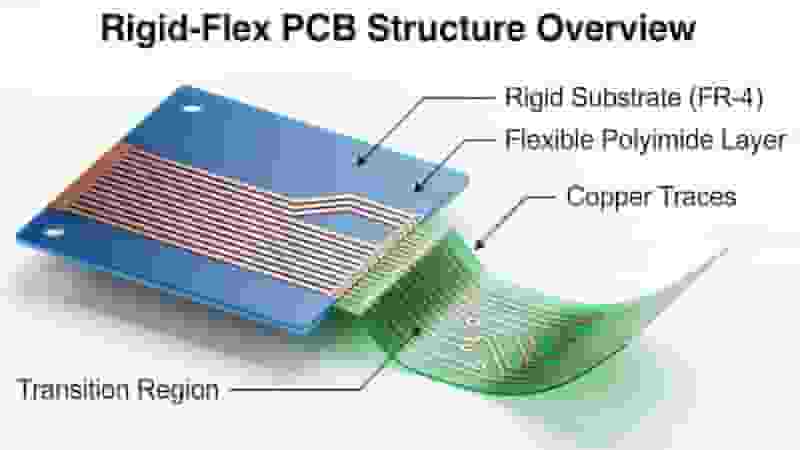
Single Layer Rigid-Flex PCB
Combines rigid and flexible substrates for compact devices like cameras and handheld instruments. Ideal for space‑constrained designs.
Single Layer High-Frequency PCB
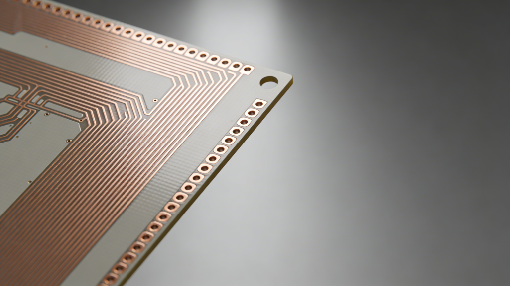
Uses Rogers or other high‑frequency materials for RF communication and signal transmission applications. Ensures excellent signal integrity.
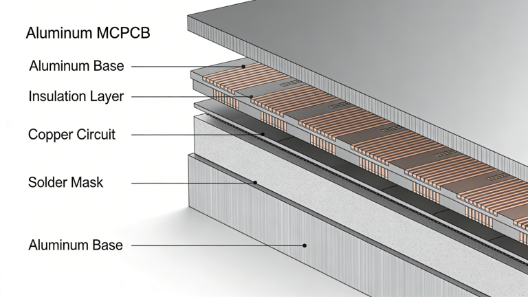
Single Layer Aluminum PCB
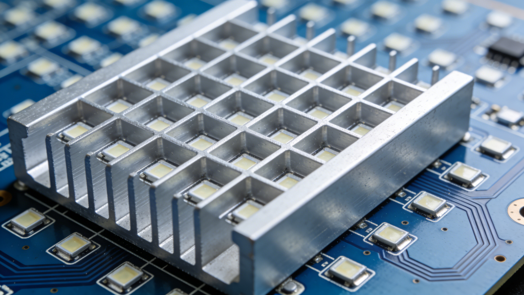
Features excellent thermal conductivity, perfect for LED lighting, power drivers, and heat‑sensitive equipment.
Benefits of Single Layer PCBs
Cost‑Effective: Lowest production cost among all PCB types, ideal for high‑volume projects.
Simplified Production: Single copper layer reduces defects and shortens lead times.
High Reliability: Simple structure delivers stable performance in harsh environments.
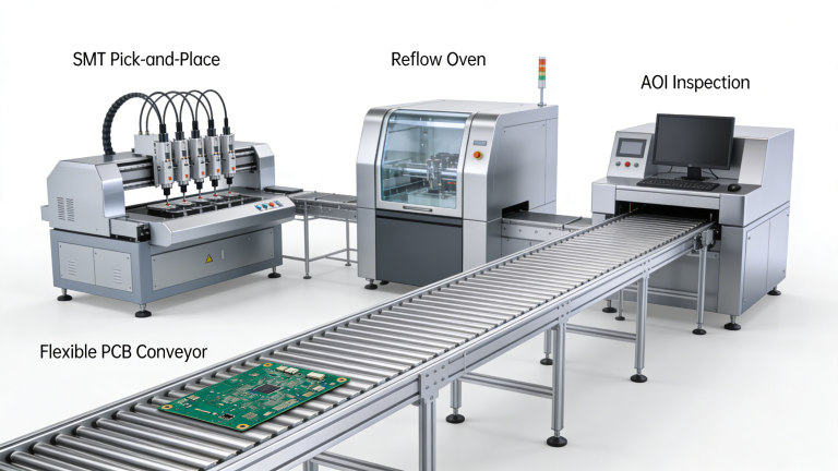
Easy Testing & Assembly: Convenient for AOI, electrical testing, and manual or automated assembly.
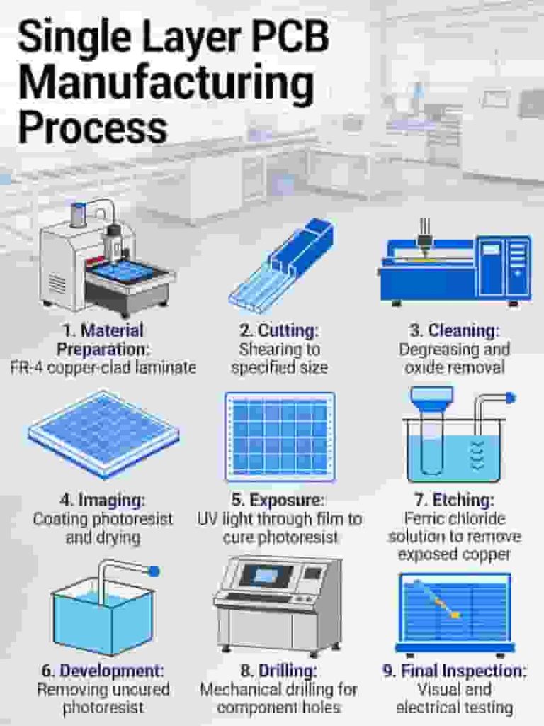
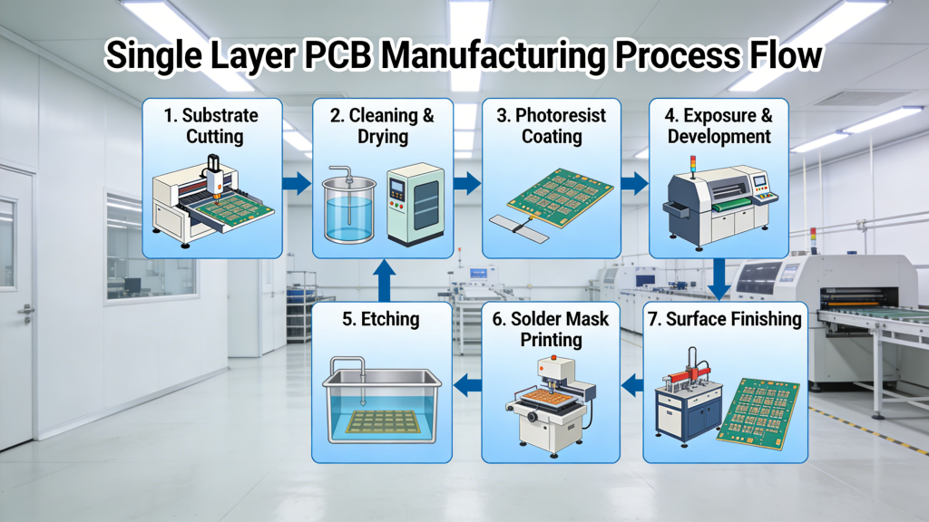
Single Layer PCB Manufacturing Process
1. Order & DFM Check: Review Gerber files to optimize design for manufacturability.
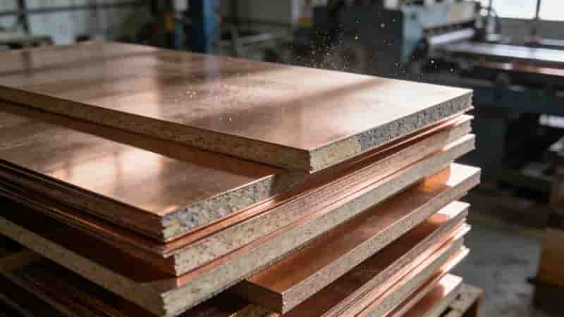
2. Material Preparation: Cut base materials to required panel size.
3. Circuit Printing & Etching: Transfer and etch copper circuits accurately.
4. Drilling: Create precise holes for components.
5. Solder Mask & Silkscreen: Apply protective coating and identification printing.
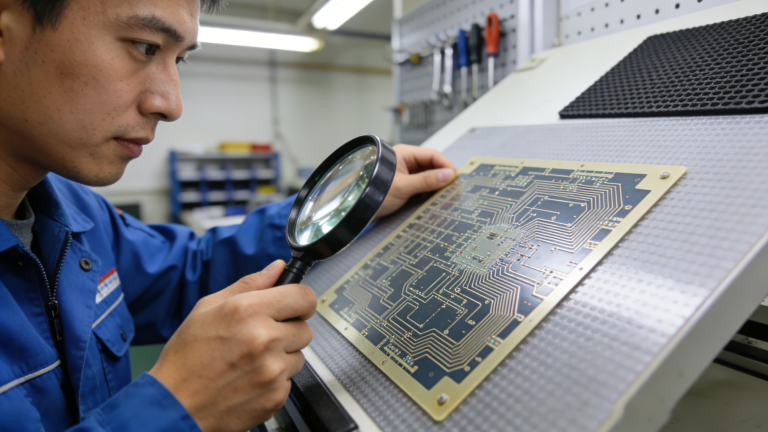
6. Electrical Testing & Inspection: Ensure 100% quality before shipment.
Single-Sided vs Double-Sided vs Multilayer PCBs
| Feature | Single-Sided PCB | Double-Sided PCB | Multilayer PCB |
|---|---|---|---|
| Conductive Layers | 1 | 2 | 3+ |
| Typical Cost | Low | Moderate | High |
| Complexity | Simple | Moderate | High |
| Main Applications | LED, power supplies, consumer electronics | Industrial controls, automotive | Aerospace, medical, high‑tech devices |
Summary
Single layer PCB manufacturing provides the most economical and reliable solution for simple electronic devices. With multiple material options and a streamlined production process, single sided PCBs are widely used in lighting, power, and consumer electronics. We support rapid prototyping, mass production, and free DFM checks to ensure your project success.
Need High-Quality & Affordable Single Layer PCBs?
Request a free quote, free DFM analysis, and custom solutions today.
Get Your Free Quote Now
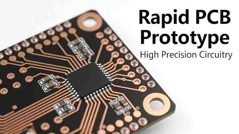
Accelerate Your Innovation with Rapid PCB Prototyping
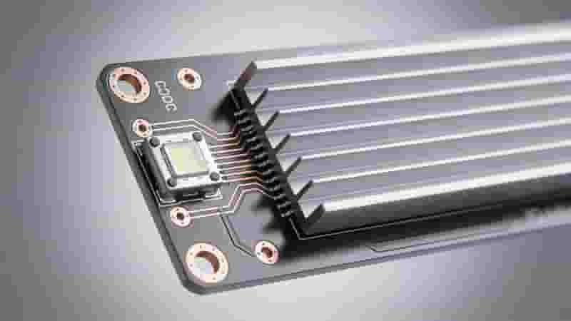
Copper Clad Laminate (CCL): The Complete 2026 Guide for PCB Manufacturing
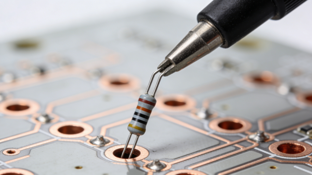
Through-hole PCB Assembly Service | IPC Certified THT PCBA Solutions
PCB Manufacturing Process Part 1: MI, Cutting & Drilling – Complete Industrial Guide
Automotive Printed Circuit Boards: Reliable Solutions for Vehicle Electronics