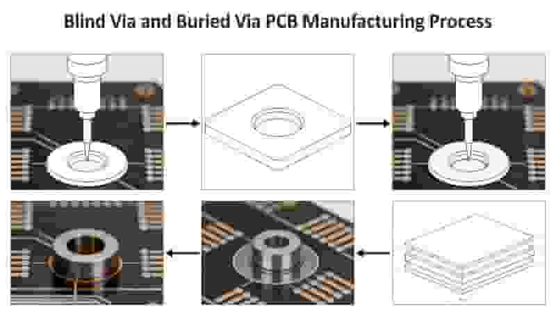
Blind vias and buried vias are core structures for high‑density interconnect (HDI) and high‑speed PCBs. They boost routing density, signal integrity, and miniaturization while optimizing layer stackups. This guide covers definitions, differences, design rules, manufacturing, and industrial applications for global engineers and buyers.
Introduction
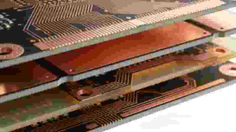
As printed circuit boards become more compact and integrated, advanced via structures replace traditional through‑hole vias to meet complex routing demands. Blind vias and buried vias solve limitations of PTHs in multilayer, high‑speed, and miniaturized designs.
These vias improve density, signal quality, and stackup efficiency. Understanding their use is critical for engineers, procurement teams, and manufacturing partners building reliable, cost‑effective electronics.
What Are Blind Vias in PCBs?
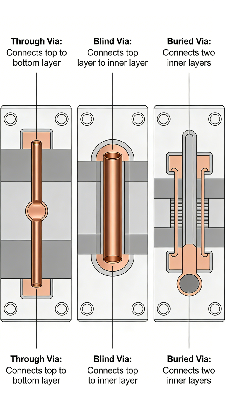
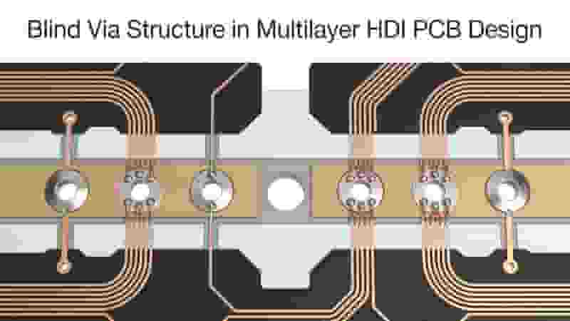
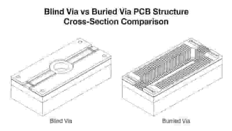
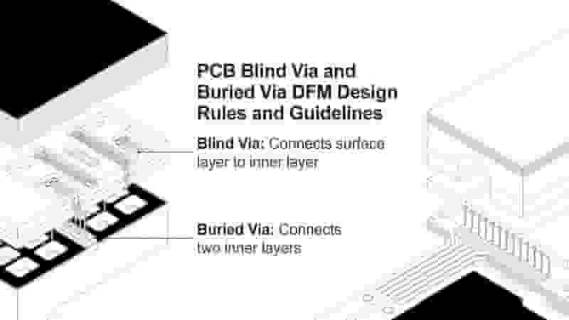
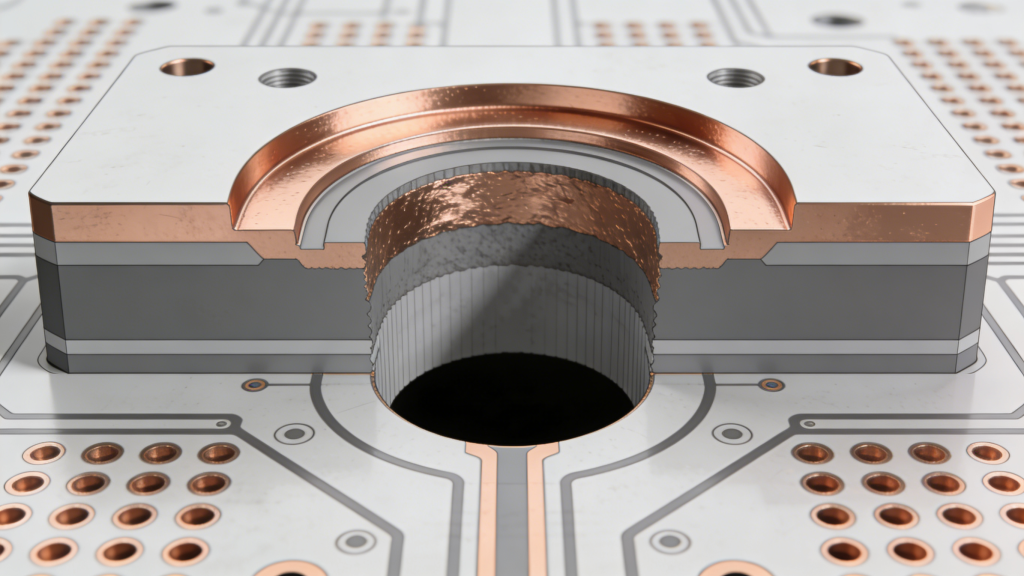
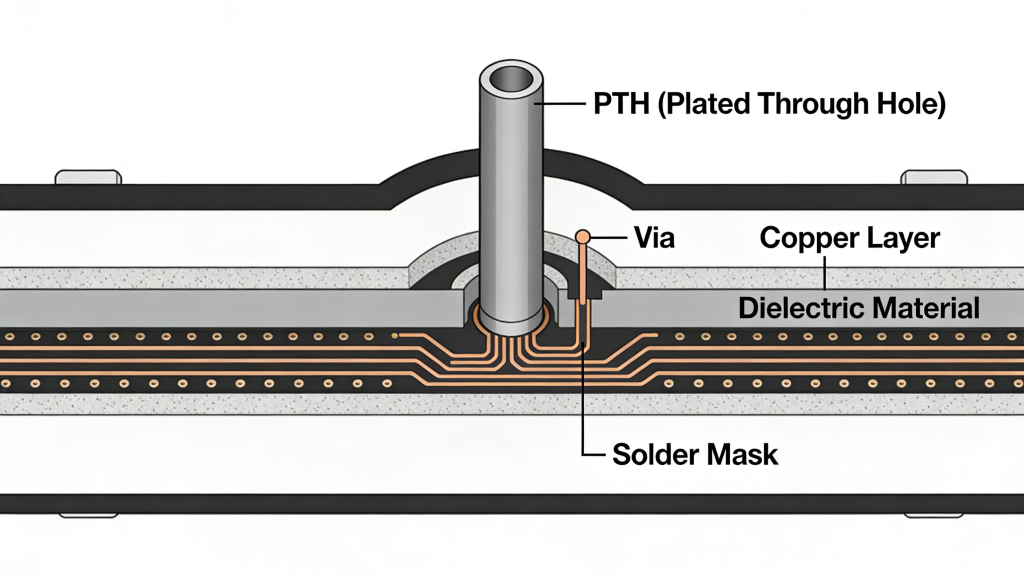
A blind via is a plated hole connecting one outer layer to one or more inner layers without passing through the entire board. It is visible from one side only and terminates at a target inner layer.
Key Characteristics:
- Connects one outer layer to inner layers
- Does not penetrate the full PCB stackup
- Smaller diameter than standard PTHs
- Common in HDI and >4‑layer boards
Main Benefits:
- 15–20% higher component density
- Flexible routing in dense layouts
- Lower lamination and material cost
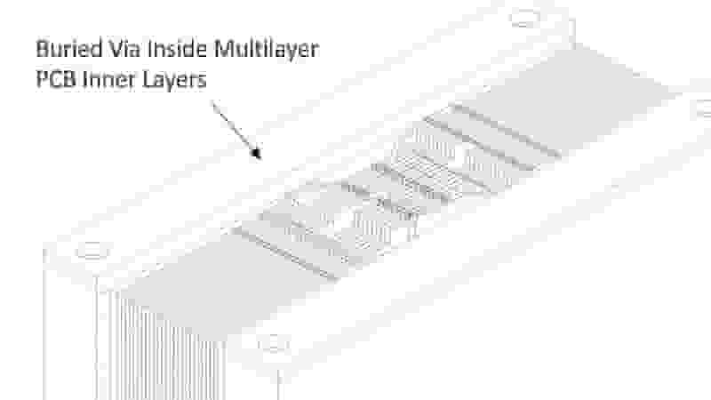
What Are Buried Vias in PCBs?
A buried via links two or more inner layers only, with no connection to either outer layer. It is fully embedded inside the PCB and invisible after lamination.
Key Characteristics:
- Connects only internal layers
- No exposure on top or bottom surfaces
- Requires sequential lamination
- Ideal for high‑layer‑count boards
Main Benefits:
- Improved signal integrity for high‑speed designs
- Lower parasitic capacitance
- Full outer‑layer space preservation
- Reduced electromagnetic interference
Blind Vias vs Buried Vias – Full Comparison
| Item | Blind Vias | Buried Vias |
|---|---|---|
| Connection | Outer layer ↔ Inner layer | Inner layer ↔ Inner layer only |
| Visibility | Visible from one side | Fully hidden |
| Inspection | Visual & probe test allowed | X‑ray only |
| Best For | BGA fanout, HDI, cost savings | High‑speed, RF, high layer counts |
Design & Manufacturing Considerations
Using blind vias and buried vias requires strict DFM rules to ensure yield, reliability, and cost control:
- Manufacturers need precise drilling and layer registration (±0.002” or better)
- Additional lamination steps increase cycle time
- X‑ray inspection is required for buried structures
- Follow minimum annular ring, spacing, and aspect ratio guidelines
- Thermal stress and reliability testing are critical
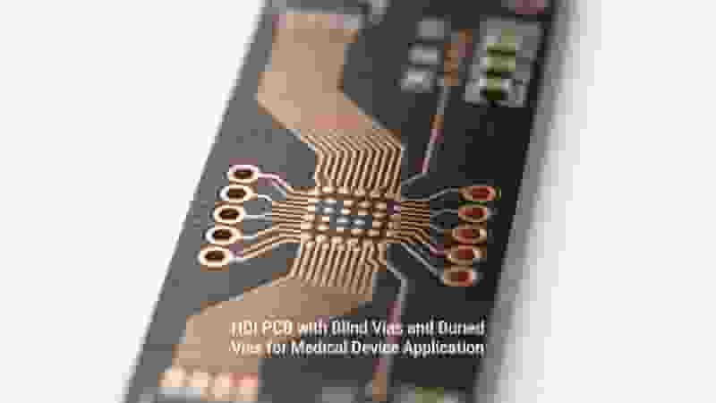
Key Applications of Blind Vias & Buried Vias
These vias are widely used in high‑performance electronics:
- HDI PCBs: Increase wiring density by over 20%
- High‑speed digital circuits: Improve signal integrity and reduce parasitics
- RF & microwave designs: Control impedance and reduce interference
- Automotive electronics: High integration and reliability
- Wearable & portable devices: Enable extreme miniaturization
Conclusion
Blind vias and buried vias are essential for modern multilayer, high‑speed, and miniaturized PCBs. They deliver better density, signal performance, and design flexibility than traditional PTHs.
Success depends on clear design rules, reliable manufacturing, and close collaboration between engineering and production teams.
Get Custom PCB Solutions with Blind Vias & Buried Vias
We specialize in HDI, high‑speed, and multilayer PCBs with precision blind vias and buried vias for global industrial clients.
Request a Quote
Contact Us for Custom Design
Understanding Plated Half-Holes (Castellated Holes) in PCB Design
How to Solder on PCB: Essential Techniques and Best Practices for Reliable Assembly
Rapid PCB Prototyping and Production: Accelerate Your Product Launch

PCB Components Purchasing Services | Global Electronic Components SourcingPCB
What is the Difference Between PTH and Via in PCBs?