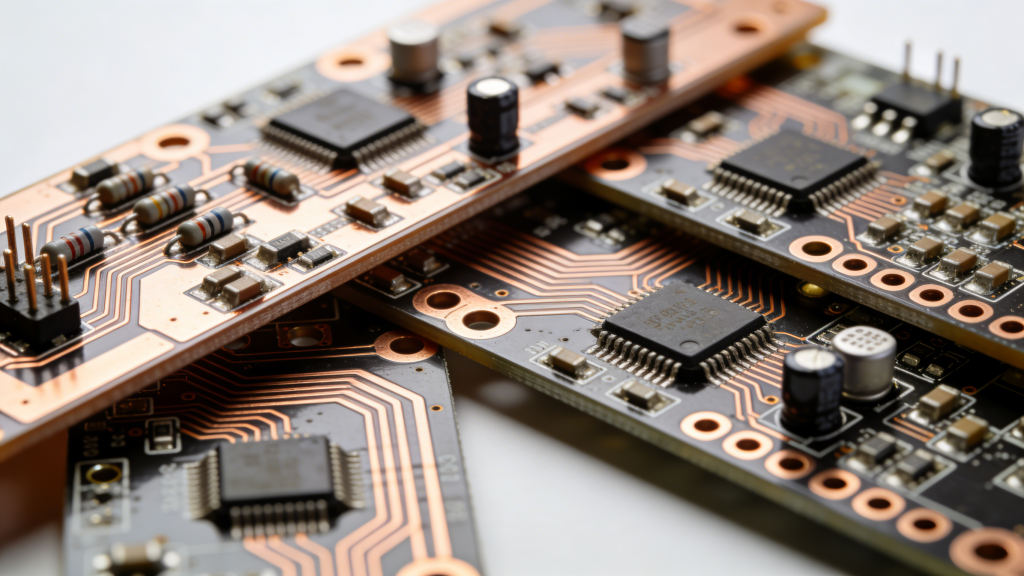
We provide custom heavy copper PCB and thick copper PCB solutions up to 12oz for high‑current, high‑thermal power electronics, automotive, industrial, and military applications. As a professional heavy copper PCB manufacturer, we deliver engineering‑driven fabrication with optimized stackups, reliable plating, and robust solder mask for long‑term performance under high current and harsh environments. Prototypes and small to medium production runs are all supported.
What Is a Heavy / Thick Copper PCB
A heavy copper PCB, also known as a thick copper PCB, is a printed circuit board with much thicker copper layers than standard PCBs. Standard boards use 0.5–3 oz/ft² copper, while heavy copper PCB starts from 3–4 oz/ft² and can reach 20 oz/ft² or higher for extreme copper designs.
Thicker copper layers enable higher current carrying capacity, better thermal dissipation, and stronger mechanical strength at connectors, vias, and high‑stress areas. This makes thick copper PCB ideal for high‑power, high‑reliability applications including power supplies, motor drives, automotive systems, and industrial equipment.

Typical Copper Thickness Comparison
| Type of PCB | Copper Thickness (per layer) | Typical Applications |
|---|---|---|
| Standard PCB | 0.5–3 oz/ft² | Consumer electronics, low‑medium power |
| Heavy / Thick Copper PCB | 3–20 oz/ft² | Power supplies, automotive, industrial |
| Extreme Copper PCB | 20–200 oz/ft²+ | High current bus bars, military systems |
Key Benefits of Heavy Copper PCB
High current carrying capability
Heavy copper PCB traces and planes increase conductor cross‑section, allowing high currents without excessive temperature rise or voltage drop, critical for power supplies, inverters, and motor drives.
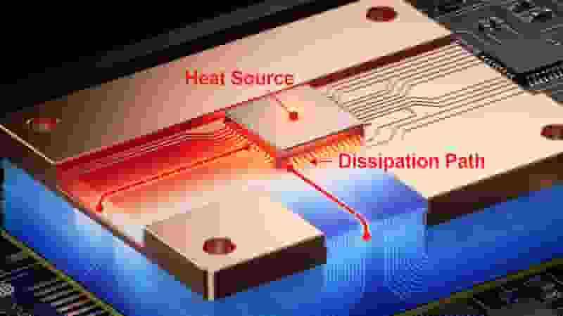
Improved thermal management
Thick copper layers act as efficient heat spreaders, drawing heat away from MOSFETs, IGBTs, and power components. This reduces thermal stress and lowers reliance on large heat sinks.
Higher mechanical strength & reliability
Reinforced pads, vias, and connectors improve resistance to thermal cycling, vibration, and mechanical shock, ideal for automotive, industrial, and military environments.
Higher power density & compact design
Integrated high‑current paths eliminate external bus bars and cables, enabling smaller, lighter, and more integrated power modules.
Stable performance in harsh environments
Robust plating and thick copper ensure long‑term reliability under high temperature, humidity, and mechanical stress for mission‑critical equipment.
Heavy Copper PCB Industries & Applications
Thick copper PCB supports high‑power and harsh‑environment applications where standard PCBs cannot meet current, thermal, or reliability requirements.
Power Supplies & Power Conversion
AC‑DC, DC‑DC power supplies, rectifiers, and high‑current power distribution units.
Motor Drives & Industrial Control
Servo drives, frequency converters, and industrial control modules with high phase currents.
Automotive & Electric Vehicles (EV/HEV)
Onboard chargers, DC‑DC converters, battery management systems, and power distribution.
Renewable Energy & Energy Storage
Solar inverters, wind converters, UPS, and energy storage systems.
High‑Current Bus Bars & Power Distribution
Integrated PCB bus bars replacing traditional copper bars for compact design.
Military, Aerospace & Heavy Industry
Shock‑resistant, high‑reliability boards for defense, rail, and heavy machinery.
Our Heavy Copper PCB Manufacturing Capabilities
We offer full‑featured heavy copper PCB fabrication with engineering support to optimize stackup, copper weight, and thermal performance.
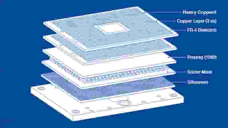
Copper Thickness & Design Parameters
| Item | Specification |
|---|---|
| Outer layer copper | 3–12 oz/ft² |
| Inner layer copper | 3–10 oz/ft² |
| Layers | 1–32 layers |
| Board thickness | 0.8–6.0 mm |
| Materials | FR4, High Tg FR4, Halogen‑free, Aluminum, Hybrid |
| Surface finishes | ENIG, ENEPIG, Immersion Silver, Immersion Tin, OSP, HASL |
DFM Guidelines for Heavy Copper PCB
Thick copper PCB requires special design rules for plating, etching, and solder mask. Follow these guidelines for stable manufacturing and cost efficiency.
1. Use wider traces and spacing as copper weight increases to ensure etching quality.
2. Apply larger via diameters and thicker plating for high‑current interlayer connections.
3. Optimize thermal reliefs and oversized pads to prevent solder cracking under thermal cycling.
4. Provide sufficient solder mask clearance to avoid bridging on thick copper profiles.
5. Select high‑Tg materials and balanced stackups to control warpage in high‑power designs.
Heavy Copper PCB Prototype & Production Service
We support full‑cycle heavy copper PCB projects from rapid prototyping to series production.
Prototyping
Flexible quantities from sample pieces to pilot runs; quick turnaround with engineering DFM review.
Small & Medium Production
Stable process control, 100% electrical testing, and consistent quality for volume orders.
Why Choose Our Heavy Copper PCB Service
• Specialized expertise in heavy copper PCB plating and etching processes
• Professional DFM engineering support to optimize your design
• Strict quality control and IPC standard compliance
• Flexible order volumes and reliable global delivery
Summary
Heavy copper PCB and thick copper PCB are essential for high‑current, high‑thermal, and high‑reliability power electronics. We provide professional manufacturing, engineering support, and flexible services for global industrial buyers, automotive suppliers, and military contractors. From prototype to production, we deliver reliable heavy copper PCB solutions that meet your performance and quality requirements.
Request Your Heavy Copper PCB Quote Now
Upload your Gerber files for a free DFM check and get a professional quotation for your heavy copper PCB project.
Get Heavy Copper PCB Quote
Upload Gerber for Free DFM
Flying Probe Testing for PCB: The Complete Professional Guide
How to Use PCB Stencil: Professional Step-by-Step Guideline
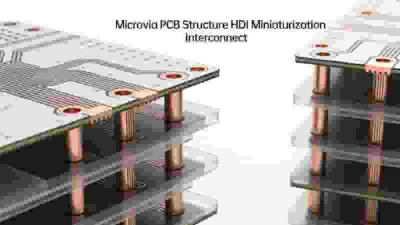
Microvias in PCBs: Complete Technical Guide for HDI & Miniaturization
SMT PCB Assembly Services for Prototypes & Production
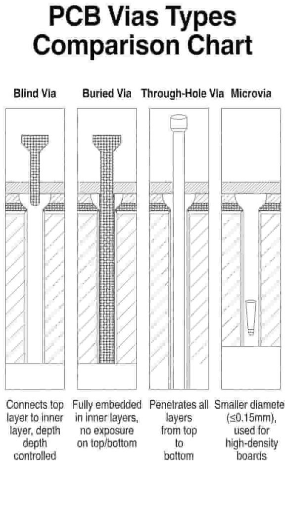
PCB Vias: Complete Overview, Types, Design & Manufacturing for Engineers & Buyers