|

Immersion Silver PCB Surface Finish: Benefits, Applications, Cost Analysis & IPC Standards

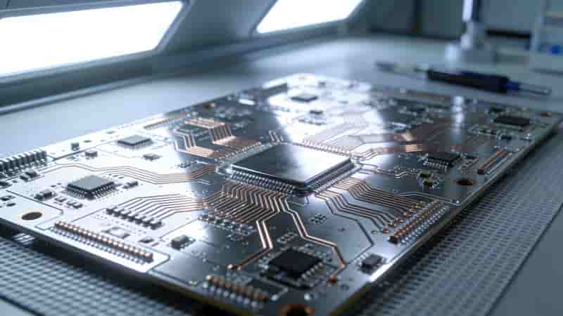
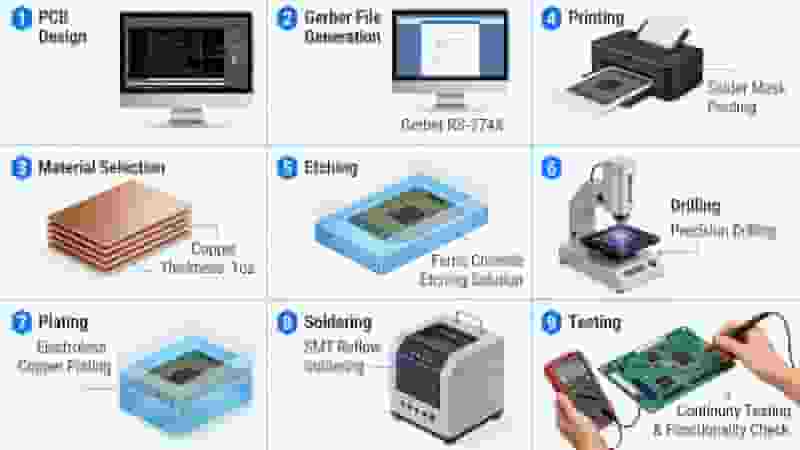
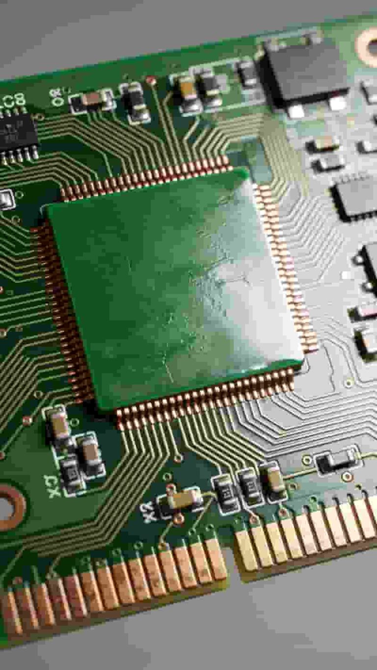
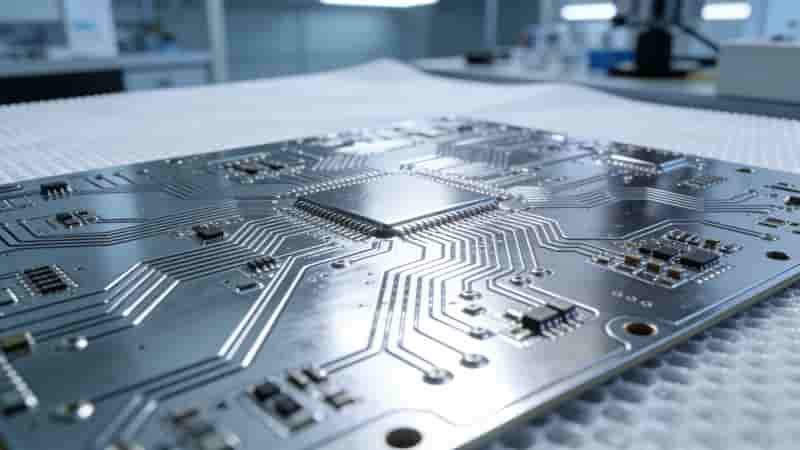
Immersion silver PCB chemical deposition process diagram

Immersion silver PCB surface finish is a lead‑free, RoHS‑compliant protective layer for copper pads, delivering balanced cost, solderability, and high‑speed signal performance. Widely used in telecom, automotive, and fine‑pitch electronics, it offers a practical alternative to ENIG and HASL. This guide covers process, pros & cons, applications, cost data, and side‑by‑side comparisons for engineering and procurement teams.

What Is a PCB Surface Finish?

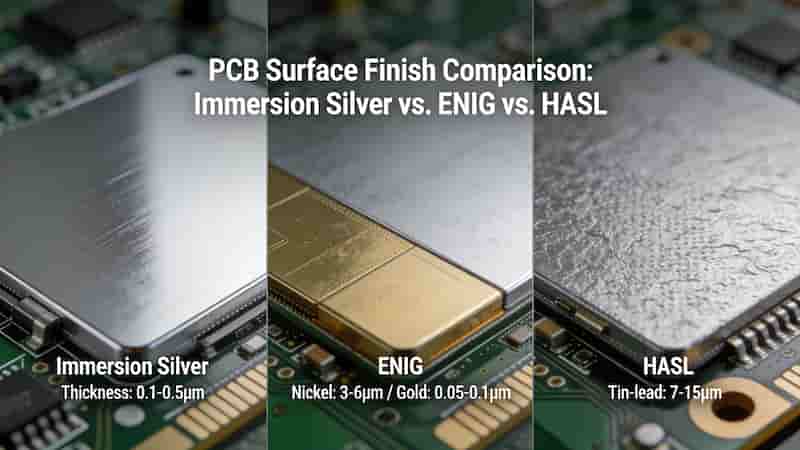
A PCB surface finish protects exposed copper from oxidation, improves solderability, and secures component bonding. Common types include immersion silver PCB surface finish, ENIG, HASL, OSP, and immersion tin. Each differs in cost, durability, shelf life, and suitability for high‑speed or fine‑pitch designs.
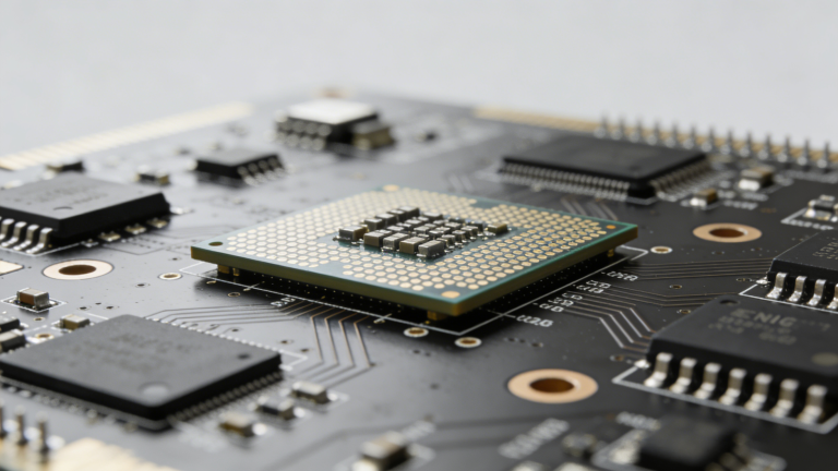
PCB surface finish types comparison including immersion silver, ENIG, HASL for PCB manufacturing

How Does Immersion Silver Work?

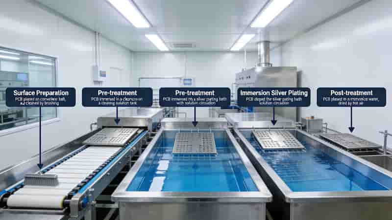
Immersion silver PCB surface finish uses a chemical displacement reaction: silver ions replace surface copper atoms to form a uniform layer of 5–18 µin (0.125–0.45 µm).

Process steps:

  1. Micro‑etching to improve adhesion
  2. Silver deposition at 40–60°C, pH 4–6
  3. Anti‑tarnish treatment for extended shelf life

Reaction: Cu + 2Ag⁺ → Cu²⁺ + 2Ag

IPC data shows immersion silver PCB holds 15% of global surface finish usage due to cost‑performance balance.
Immersion silver PCB chemical deposition process diagram

Key Benefits of Immersion Silver PCB Surface Finish

  • Cost efficiency: 20–30% lower than ENIG for 2–layer boards
  • Superb solderability: Uniform wetting reduces assembly defects
  • RoHS & lead‑free: Compliant with global environmental standards
  • Multiple reflows: Stable for 3–5 thermal cycles
  • High conductivity: Ideal for 5G, RF, and high‑speed signals
  • Flat surface: Supports fine‑pitch components (0402, 0201, QFN)
  • No black pad risk: More reliable than ENIG in critical assemblies

Limitations & Mitigation

While immersion silver PCB surface finish performs well, it has manageable weaknesses:

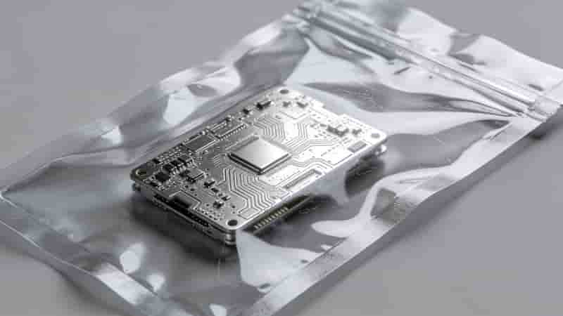
  • Tarnishing in sulfur or high humidity → vacuum packing extends shelf life to 6–12 months
  • Potential micro‑voids in high moisture → controlled assembly environment
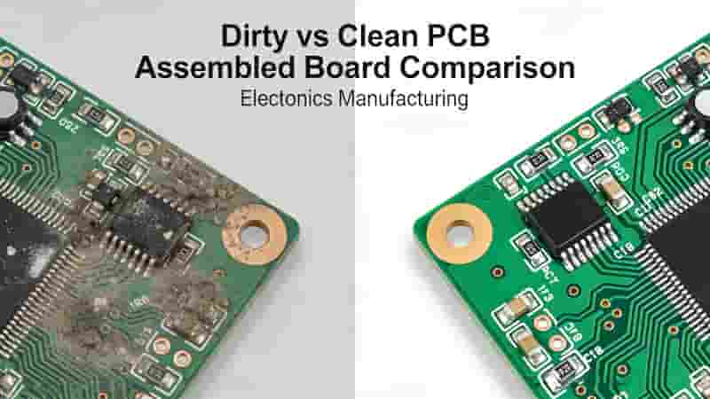
  • Handling sensitivity → ESD‑safe processing and clean assembly
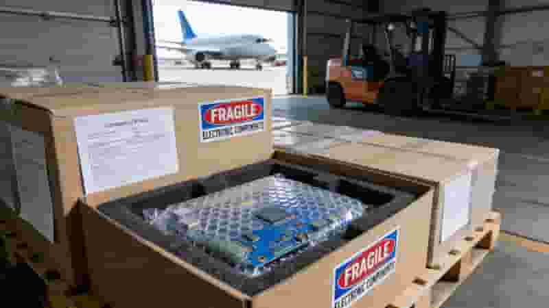
Immersion silver PCB tarnish protection and storage method

Industry Applications

Immersion silver PCB fits high‑performance, cost‑conscious industries:

  • Telecom: 5G base stations, RF modules, high‑speed routers
  • Automotive: ADAS, EV controllers, radar sensors
  • Consumer electronics: Smartphones, wearables, tablets
  • Medical: Diagnostic tools, imaging equipment
  • Aerospace: Satellite communication modules

Immersion Silver vs ENIG vs HASL Comparison

FeatureImmersion SilverENIG (Immersion Gold)HASL
Cost20–30% cheaper than ENIGHighLowest
Shelf Life6–12 months (sealed)12+ months6–12 months
SolderabilityExcellentExcellentGood
Fine‑Pitch FitExcellentExcellentPoor
RoHSCompliantCompliantLeaded: Non‑compliant
Immersion silver vs ENIG vs HASL PCB surface finish comparison chart

How to Choose a Reliable Immersion Silver PCB Manufacturer

To ensure consistent immersion silver PCB surface finish quality, look for:

  • IPC‑4553 certified process
  • XRF thickness testing
  • Automated deposition lines
  • DFM support for high‑speed designs
  • Quick quotes and flexible lead times

We provide IPC‑compliant fabrication, strict quality control, and full engineering support for immersion silver PCB projects worldwide.

Conclusion

Immersion silver PCB surface finish is a cost‑effective, high‑performance solution for modern electronics. It excels in high‑speed signal integrity, fine‑pitch compatibility, and RoHS compliance, making it a top choice for telecom, automotive, and consumer devices. With proper storage and manufacturing control, it delivers reliable performance at a lower cost than ENIG.

Start Your Immersion Silver PCB Project

Get a fast, detailed quote for immersion silver PCB manufacturing & assembly. Send your Gerber files or BOM for professional evaluation.
Request a Free Quote

Immersion silver PCB manufacturing and assembly service for global buyers
SMT Stencil Selection Guide for PCB Engineers

Ultimate Guide to SMT Stencils: Types, Selection & Best Practices for PCB Assembly

Posted on
0 Comments
SMT stencils are critical for precise solder paste deposition in PCB assembly. This complete guide covers types, materials, selection tips, and pro techniques to improve yield and reliability for engineers and global buyers. What Is an SMT Stencil? An SMT stencil is a thin precision metal sheet (usually stainless steel) with laser‑defined apertures that control…
PCB Stencil Quality Control Inspection

High-Precision PCB & SMT Stencil Manufacturing

Posted on
0 Comments
Professional high-precision PCB and SMT stencil manufacturing services for global electronics manufacturers. Custom laser-cut stencils, strict quality control, fast delivery, and full compliance with IPC standards. What Are PCB and SMT Stencils for SMT Assembly PCB stencils (also called SMT stencils) are precision-engineered stainless steel tools used to apply solder paste accurately onto printed circuit…
PCB Component Spacing vs Height Layout Guidelines

PCB Pad Design Basics: Standards, Rules & Best Practices for Engineers

Posted on
0 Comments
This guide covers core PCB pad design principles, component spacing, IPC standards, SMD/through-hole rules, thermal management, and DFM to boost assembly yield, reliability, and performance for industrial and export-grade PCBs. PCB Component Layout & Spacing Rules When laying out PCB components, designers must balance minimum component spacing against component height and thickness. Proper spacing prevents…
Single Layer PCB Manufacturing Process Flow Chart

Single Layer PCB Manufacturing | Affordable Single Sided PCBs

Posted on
0 Comments
We provide professional single layer PCB manufacturing with ISO-certified quality, fast lead times, cost-effective pricing and free DFM analysis for global industrial buyers, engineers and importers. Our single sided PCBs are widely used in LED lighting, power supplies, consumer electronics and industrial control equipment. What Is a Single Layer PCB A single layer PCB (also…
Fast Turnaround PCB Prototype Manufacturing Line HDI Microvias

Fast Turnaround PCB Prototype Services from Certified Manufacturer

Posted on
0 Comments
Quick turn PCB prototyping, custom solutions for startups and enterprises. ISO-certified, rapid delivery, and global support – upload your design for a free DFM check! ✅ As fast as 24-hour build and delivery ✅ No minimum quantity ✅ IoT, automotive, medical, consumer electronics Get Instant QuoteUpload Gerber Files Contents Why Rapid PCB Prototyping for Every…
Quick Turn PCB Prototype Assembly Process

Quick Turn PCB Assembly Services for Fast Prototypes and Production

Posted on
0 Comments
Get reliable quick turn PCB assembly with one-stop PCB fabrication, components sourcing, SMT/THT assembly and testing, helping you turn ideas into working boards in days instead of weeks. What Is Quick Turn PCB Assembly Service? Quick turn PCB assembly is an accelerated manufacturing process that integrates PCB fabrication, component sourcing, SMT/THT assembly and testing to…

FAQs About Immersion Silver PCB Surface Finish

A: It is a lead-free, RoHS-compliant coating formed by chemical displacement reaction, protecting copper from oxidation and ensuring great solderability and high conductivity.

A: Cost 20-30% lower than ENIG, flat surface for fine-pitch parts, excellent conductivity for high-speed/RF circuits, no black pad issue and supports multiple reflows.

A: It may tarnish in humid or sulfur-rich environments. Use vacuum packaging and ESD-safe handling to extend shelf life to 6–12 months.

A: It costs less than ENIG and has better fine-pitch performance than HASL. HASL is the cheapest but not ideal for tiny components.

A: Widely used in 5G telecom, automotive electronics, consumer gadgets, medical devices and aerospace communication modules.

A: Normally 6 to 12 months when sealed in vacuum packaging under proper storage conditions.

A: Production follows IPC-4553 standard, with XRF thickness testing and automated production lines to guarantee stable coating quality.

A: Yes. Its ultra-flat surface works well with 0402, 0201 chips, QFN and other fine-pitch packages.

Similar Posts