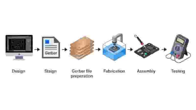
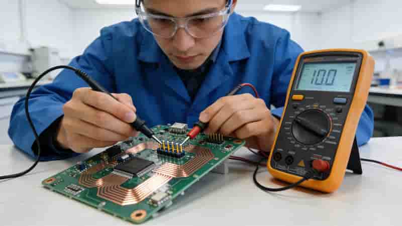
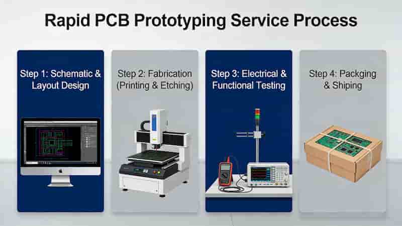
Rapid PCB prototyping allows functional validation of printed circuit board layouts within 24–120 hours. Rapid PCB prototyping services enable engineers to quickly design and manufacture printed circuit board prototypes within an extremely short timeframe, usually 1–5 days.
What Is Rapid PCB Prototyping
Rapid PCB prototyping refers to the design and manufacturing of printed circuit boards within an extremely quick timeframe, usually 1–5 days. It enables engineers to validate their PCB layouts in a timely manner instead of waiting weeks for fabrication through standard processes.

Rapid PCB prototype service features include:
- Fast turnaround time: Extremely fast turnaround time: Rapid PCB prototypes delivered in just 24–120 hours
- Low startup costs for rapid PCB prototyping: Affordable pricing with flexible small-batch quantities reduces upfront costs during the critical concept verification phase.
- Quick design modifications for rapid PCB prototypes: Engineers can easily implement improvements between iterations, enhancing PCB performance, quality and reliability.
- Manufacturing process validation: Software layouts can be assessed under real-world production procedures via the prototyping stage before final mass production.
Rapid PCB prototyping gives product designers the tremendous advantage of evaluating and refining working models early in development without slow production delays. This allows for cost and risk reduction while accelerating time-to-market.
Applications of Rapid PCB Prototypes
Rapid PCB prototyping services enable engineers to validate concepts, pinpoint design flaws, and optimize performance in printed circuit board layouts long before mass production.
Proof of Concept Testing
Building low-cost, quick-turn prototypes allows verification that a proposed PCB design performs required functions as expected during initial concept testing phases. This confirmation de-risks further development investments for inventors and entrepreneurs when launching new products.
Faster Design Iterations
Rapid PCB prototypes facilitate accelerated learning cycles, with layouts refined over successive versions. Quick-turn PCB prototype fabrication between design iterations rapidly surfaces issues needing improvement. This promptly steers enhancements, saving critical development time and resources.
Reducing Time-to-Market
Early rapid PCB prototyping and testing enable PCB functionality confirmation while parallel product development work streams progress. This paves the way for faster market launch, without waiting months for first standard test boards. First-mover advantage is strengthened as a result.
Choosing a Rapid PCB Prototype Manufacturer
Selecting the right rapid PCB prototyping partner is crucial for accelerated product development. Engineers should evaluate suppliers on:
- True 24-Hour Delivery Capability: The contractor should have genuine quick-turn fabrication abilities, not just empty sloganeering. Confirm multiple ordering and shipping cutoffs daily for fastest build speed.
- Diverse Manufacturing Technologies Supported: Ask whether services support lower cost printed circuit board prototyping techniques like laser direct imaging (LDI), mechanical milling or chemical etching alongside conventional methods.
- Customizable Ordering Procedures: Opt for flexible, designer-centric workflows allowing PCB layout file uploads direct to order forms, not inflexible legacy systems. Prioritize agility.
- Experienced Engineering Assistance: Knowledgeable technical experts should actively guide prototyping design-for-manufacture decisions through collaborative consultation to avoid unanticipated delays.
- Reasonable Pricing on Low Quantities: Economical small-batch pricing allows more iterations. However quality, tolerances and materials should not be sacrificed only for lowest cost on quick-turn jobs.
- Rapid Multi-Iteration Abilities: Judge lead times not just on one-off builds but on entire prototyping roadmaps. Assess parallel vs sequential job efficiencies for executing the fastest iterative testing across multiple progressive design versions.
Rapid Prototype PCB Pricing & Cost Considerations
When budgeting rapid printed circuit board prototypes, engineers should understand popular pricing models in comparison to standard fabrication runs:
- Quantified by Area: Prototyping costs often utilize square inch charges encompassing smaller PCB sizes. This allows flexibility but control versus high volume aggregate board pricing.
- Less Duties & Amortizations: Rapid prototypes sidestep expenses like testing, tooling amortization and boutique duties placed on conventional orders. However, economies of scale still apply.
- Varying Across Production Techniques: Alternative rapid prototyping production technologies enable cost efficiencies but involve tradeoffs. For example, basic milling has become cost effective for simpler board geometries.
- Higher Per Unit at Low Scale: The overall expense per board drops significantly when ordering production volumes in the hundreds or thousands. So per unit pricing is higher for prototyping’s small batches.
- Total Spending Can Be Decreased: Counterintuitively, increasing rapid iteration prototyping upfront can lower total budget outlays through earlier problem discovery before mass component expenditures or fabrication investments.
Rapid Prototype PCB Quality & Testing Considerations
While rapid PCB prototypes sufficiently validate design concepts, engineers cannot expect equivalency in quality or tolerances compared to finished production boards. Instead, disciplined testing workflows should be implemented:
- Understand Dimensional Variation: Rapid prototypes involve more variance in parameters like trace widths or drill registration accuracy than established mass production processes due to faster fabrication techniques.
- Implement Functional Testing First: Focus initial testing on whether critical operating performance meets fast-paced prototyping requirements through methodical functional experimentation procedures.
- Simplify Design Rules and Standards: Relax stringent specifications during prototyping around spacing, widths or stitching unnecessarily driving up costs. But monitor electrical and RF immediacy needs.
- Lower Layer Count When Possible: Thinner, single or double layer board constructions not only accelerate fabrication but support quality consistency across quick iterations as processes stabilize.
- Appropriate Rapid Prototype Expectations: While refined for small-batch cost-effectiveness, rapid prototype PCB quality involves reasonable statistical fluctuations acceptable through product development cycles.
The Benefits of Iterating PCB Prototype Designs Quickly
Rapid PCB prototyping enables creating multiple, fast design iterations with various constructive advantages:
- Trying More Ideas: Building and testing more potential versions in compact development windows breeds bold experimentation of differentiated solutions.
- Faster Optimization: Prompt fabrication turnarounds fuel rapid integration of previous test findings into successive PCB layout adaptations, compounding improvements faster.
- Accelerated Feedback Loops: Ultra-short revision cycles permit exploratory concept tweaks transforming into quantifiable performance gains through repeatedly closing the feedback loop faster.
- Reduced Risk of Design Flaws: Incrementally checking small batches uncovers systematic issues hiding in first prototypes before volume production’s expensive sunk costs make design changes costlier.
- Greater Development Agility: Easy prototype modifications support pivoting product directions quickly while also responding faster to shifting customer needs and external market feedback.
Conclusion & Summary
In summary, rapid PCB prototyping delivers invaluable advantages through the entire electronic product development life cycle:
- Fast concept verification minimizes upfront risks for inventors progressing to first prototypes.
- Accelerated design optimization via quick revisions improves quality and performance cost effectively.
- Faster feedback loops foster critically responsive engineering and manufacturing enhancements.
- Quick-turn abilities support greater marketplace adaptability and competitive robustness.
However, maximizing these rapid prototyping benefits depends on selecting an expert PCB prototyping partner offering:
- Genuine 24 hour turnaround abilities even for intricate, high layer designs
- Breadth of low and high volume specialized manufacturing technologies
- Flexible order processes with superior end-to-end technical support
- Reasonable small-batch pricing strategies
- Seamless multi-iteration design transfer capabilities
With our extensive rapid PCB prototyping expertise, we deliver across these service attributes to fuel customers’ innovation speed to market.
Ready to Start Your PCB Projects?
Get DFM-optimized boards in as fast as 24 hours. 100% quality guaranteed.
Get a Free Quote
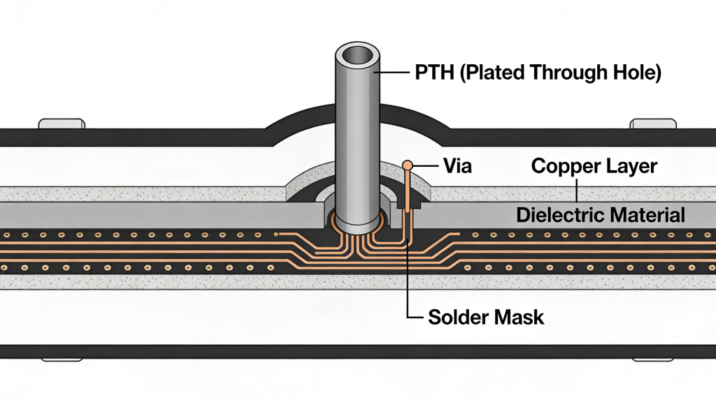
What is the Difference Between PTH and Via in PCBs?
HDI PCB Layout and Basic HDI Design Guidelines
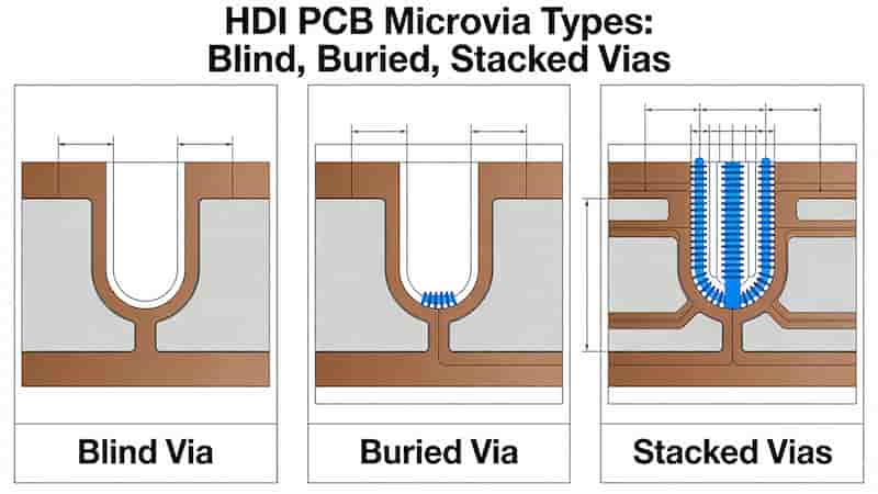
The Essentials of Microvias – Enabling Miniaturization in PCBs
Standard PCB Thickness – The Complete Guide for Engineers & Buyers
PCB Classification Guide: Types, Applications & Selection for Beginners & Pros