Summary: This professional guide covers PCB vias definitions, core types, structure, design rules, aspect ratio, annular ring, manufacturing processes, and reliability standards. It helps engineers and buyers select the right via solutions for multilayer, high-speed, and HDI PCBs to ensure signal integrity, yield, and cost efficiency.
What Are PCB Vias
A via is a vertical electrical connection between layers in a printed circuit board. Vias enable traces to transition between layers to facilitate complex routing pathways and component connections within a confined PCB area or across multilayer PCB boards.
Without reliable vias, multilayer PCBs cannot achieve layer-to-layer connectivity, leading to functional failure, signal loss, or overheating. For industrial, automotive, and high-speed applications, consistent via quality directly determines product lifespan and stability.
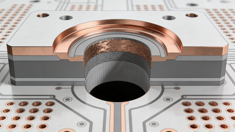
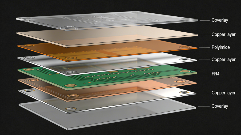
Core Structure of a Via
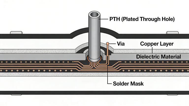
Every standard PCB via includes three key components:
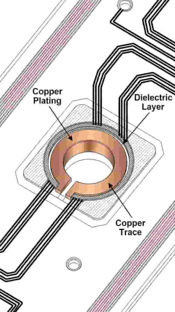
- Barrel: Copper-plated inner hole forming the main conductive path
- Pad: Copper annular ring connecting the barrel to traces or planes
- Antipad: Clearance area isolating the via from non-target layers
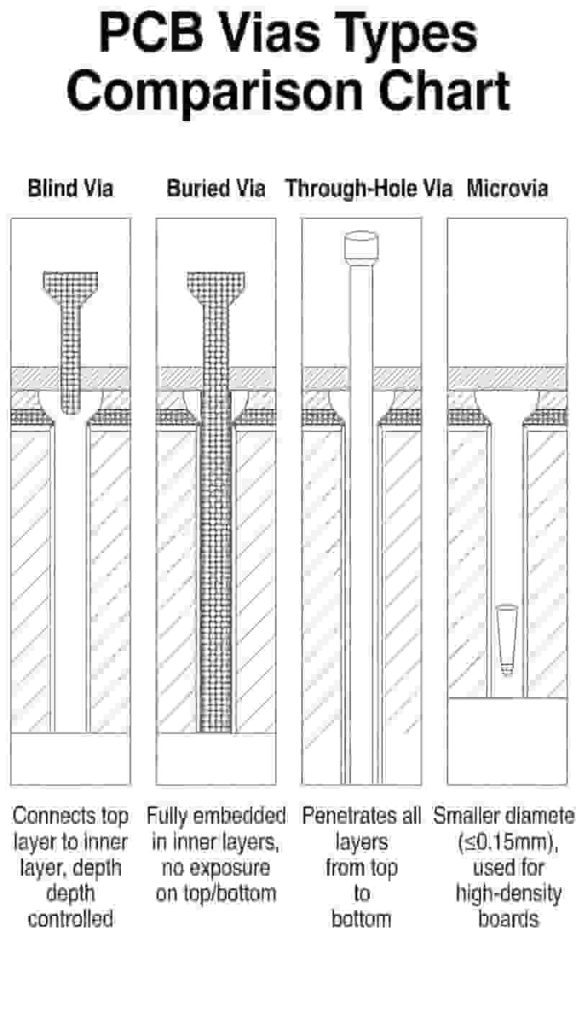
Main Types of PCB Vias
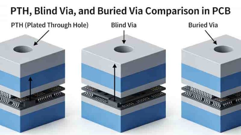
1. Plated Through-Hole Via (PTH)
Spans the full board thickness, most widely used for general circuits. Low cost, mature process, high reliability. Ideal for conventional 2–8 layer PCBs.
Partial-depth vias connecting internal layers without spanning fully through the board. Blind vias connect one internal layer to an external layer, while buried vias connect internal layers only.
3. Buried Via
Located only between inner layers, invisible externally. Maximizes routing density for high-layer-count and HDI boards.
4.Micro Vias:
Small diameter vias, typically below 0.15mm, created with laser drilling. Micro vias facilitate connections in high density PCBs.
5. Thermal Via
Designed for heat transfer from power components to inner planes. Often used in arrays to enhance cooling efficiency.
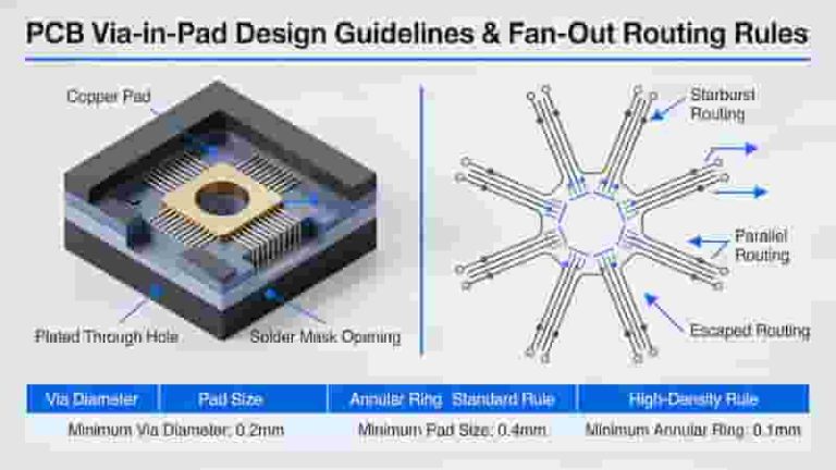
Key Design Parameters & Standards
Professional PCB via design follows strict parameters to ensure manufacturability and reliability:
- Aspect Ratio: Board thickness ÷ via diameter. Standard: 8:1–10:1; advanced up to 12:1
- Annular Ring: Min. 4–5 mil to avoid breakout and ensure connection
- Via Spacing: ≥8 mil to prevent shorts and drilling issues
- Copper Plating: Uniform thickness per IPC‑A‑600 Class 2/3
Compliance with these rules reduces defects, improves yield, and lowers overall production cost for your PCB projects.
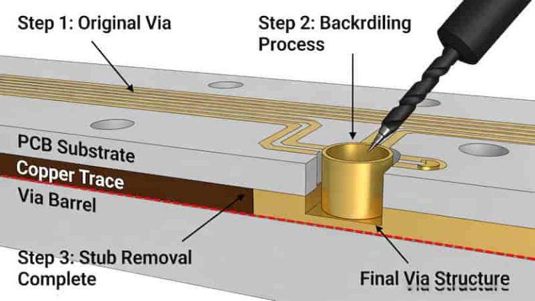
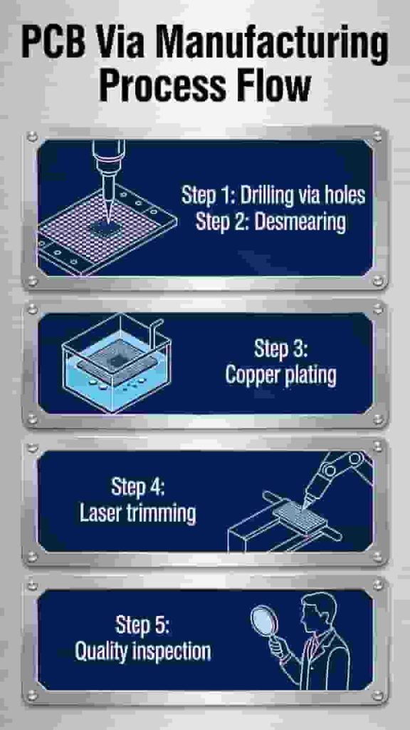
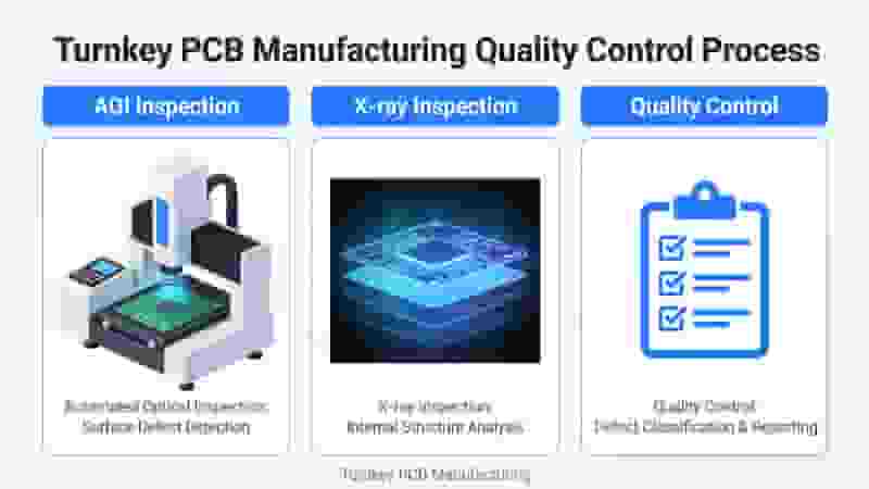
Via Manufacturing Process
- Drilling: Mechanical for PTH; laser for microvias and blind vias
- Deburring & Desmearing: Remove residues to improve plating adhesion
- Copper Plating: Form conductive barrel with consistent thickness
- Inspection: Electrical test and visual check for voids or defects
We use precision equipment and strict IPC standards to ensure every PCB via meets international quality requirements for global buyers.
Via Type Comparison Table
| Via Type | Cost | Density | Best Application |
|---|---|---|---|
| Through-Hole Via | Low | Standard | General PCBs |
| Blind Via | Medium | High | High‑Speed HDI |
| Buried Via | High | Ultra High | Multilayer Advanced |
| Microvia | High | Max | BGA, 5G, Wearables |
Conclusion
PCB vias are foundational interconnect elements that directly influence performance, reliability, and cost. Choosing the right via type and following professional design rules are critical for successful PCB development and mass production.
Whether you need standard through-hole vias or advanced microvias for HDI boards, we provide reliable manufacturing solutions that meet global industrial standards.
Need Custom PCB Via Solutions & Quotation?
Send your Gerber files and requirements for professional DFM check, via optimization, and competitive pricing for global export.
Inquire Now & Get Free Quote
Ultimate Guide to PCB Materials, Dielectric Strength, and Testing in 2025
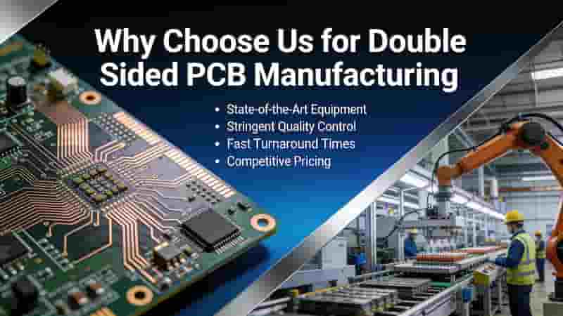
Why Choose Us for Double Sided PCBs?
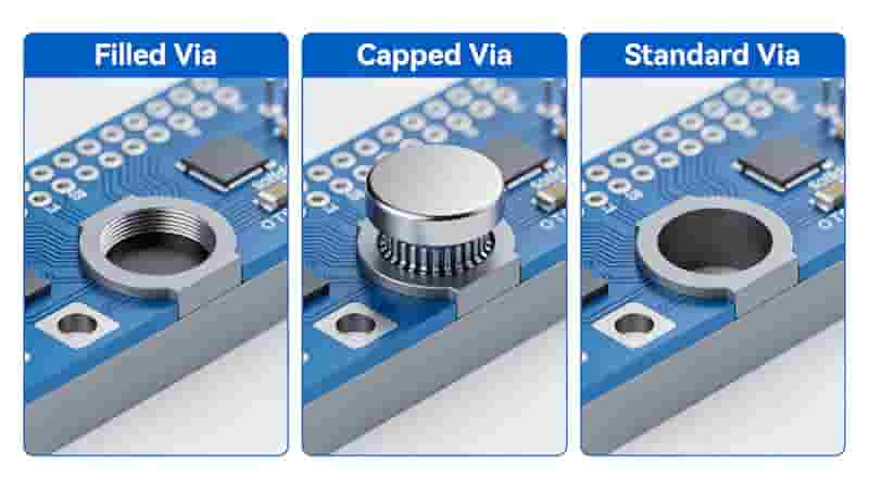
Filled and Capped Vias: Boost PCB Reliability for Industrial & Export Applications
Rigid-Flex PCB Manufacturing & Prototype Services
Turnkey PCB Manufacturing and Assembly: Full One-Stop Solution Advantages