|

Flexible Circuit Board Surface Plating: Complete Technical Guide 

Electroless Plating Process for Flexible PCB

Surface plating for flexible circuit boards is critical to solderability, oxidation resistance, bending reliability, and service life. This guide covers FPC basics, plating pretreatment, thickness control, stain prevention, electroless plating, hot air leveling, and best practices for engineers and buyers.

Flexible Circuit Board Basics

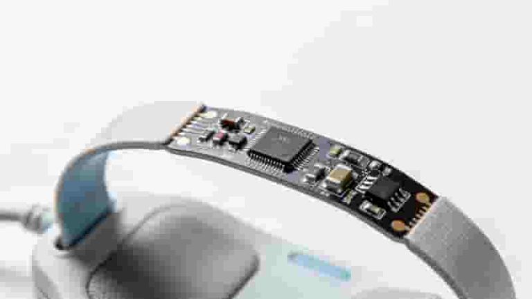
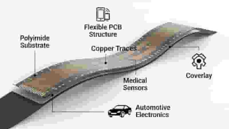
A flexible printed circuit board (FPC) uses a flexible insulating base material, enabling bending, folding, and dynamic installation. Rigid-flex PCB combines rigid PCB and flexible layers for high‑density, high‑reliability electronic devices.

Single‑sided FPC

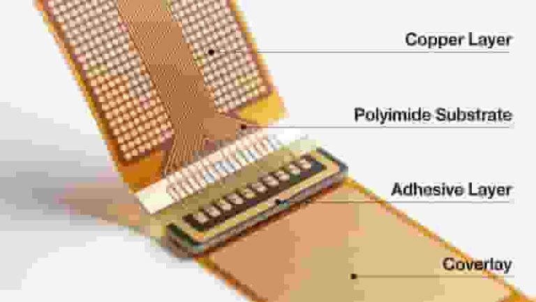
Single‑sided FPC has one conductor layer, with or without a cover layer. Common substrates: polyester, polyimide, PTFE, flexible epoxy glass cloth.

  • No cover layer: lowest cost, for mild environments
  • With cover layer: most widely used, for automotive & industrial instruments
  • Double‑sided pads without cover layer: for dual‑side component mounting
  • Double‑sided pads with cover layer: insulated, reliable for dynamic use
Single-Sided Flexible PCB Structure Diagram

Double‑sided FPC

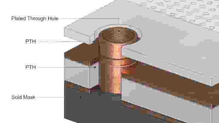
Double‑sided FPC has two conductor layers, improving wiring density. Types: with/without plated through holes, with/without cover layer.

Multilayer FPC

Multilayer FPC uses lamination technology. 4‑layer is standard (power & ground inner layers). Lighter than rigid multilayer PCB with stable electrical performance.

Multilayer Flexible PCB Structure Diagram

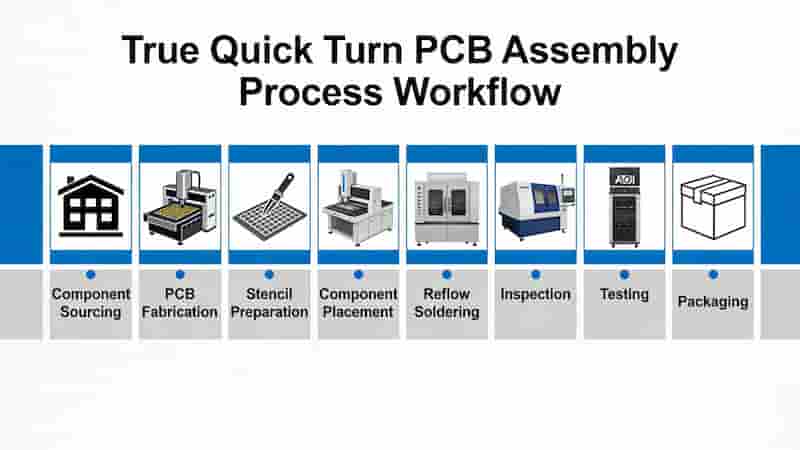
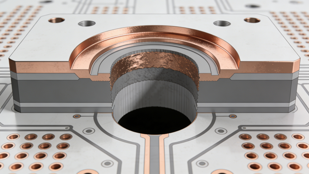
FPC Surface Plating Process

FPC plating ensures conductivity, solderability, and corrosion resistance. Key steps include pretreatment, thickness control, and cleaning.

Plating Pretreatment

Remove contaminants, adhesives, and oxides from copper surfaces. Improper treatment weakens cover layer adhesion and causes plating solution penetration.

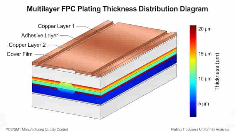
Plating Thickness Control

Thickness depends on electric field intensity: fine lines and terminal edges deposit thicker metal. Uniformity ensures consistent performance.

FPC Plating Thickness Distribution Diagram

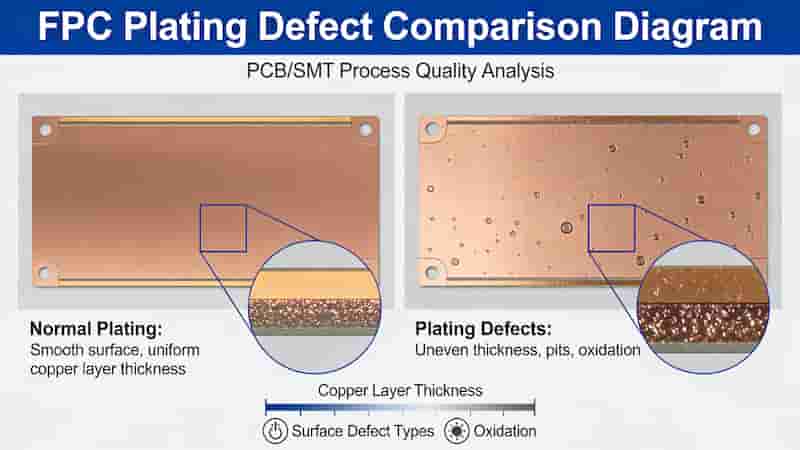
Stain & Discoloration Prevention

Residual chemicals cause post‑plating stains. Full rinsing and drying prevent discoloration. Thermal aging testing verifies cleaning quality.

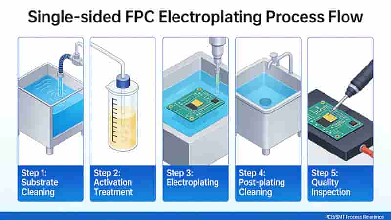
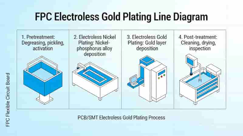
Electroless Plating for FPC

Used when conductors cannot be electrified. Typical process: electroless gold plating. High pH solutions may penetrate under cover layers; strong lamination bonding is required.

Electroless Plating Process for Flexible PCB

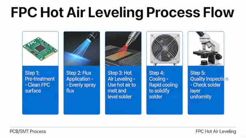
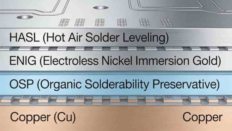
FPC Hot Air Leveling (HASL)

HASL applies molten solder then blows excess with hot air. FPC requires fixturing to avoid warping. Pre‑baking removes moisture to prevent bubbling or delamination.

ItemElectroplatingElectroless PlatingHASL
SuitabilityGeneral FPCIsolated LinesStable FPC
RiskLowMediumHigh (Delamination)
CostMediumHighLow

Summary & Best Practices

Flexible circuit board surface plating directly affects reliability. Strict pretreatment, uniform thickness, full cleaning, and proper fixturing ensure high‑quality results. Choose plating type based on application, environment, and bending requirements.

FPC Surface Plating Best Practices Flowchart

Custom Plating Service Inquiry

We provide professional flexible PCB surface plating and manufacturing services for global buyers. Get free quotation, technical support, and customized solutions for your FPC projects.

Contact us with your Gerber files, layer count, material, thickness, and quantity for a fast and accurate quote.

Request FPC Plating Quote

Cross Section of Plated Half Hole PCB

Understanding Plated Half-Holes (Castellated Holes) in PCB Design

Posted on
0 Comments
Plated half-holes, also called castellated holes, provide a space-efficient way to interconnect separate PCB modules by soldering. Unlike bottom pads, their edge positioning simplifies mounting and enhances reliability. This article explains everything about plated half-hole structures, design guidelines, manufacture, benefits and use cases. Structure of Plated Half-Holes Plated half-holes, also known as castellated holes, resemble…
How to use PCB DFM analysis step by step

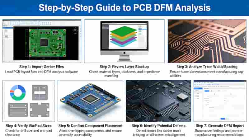
Free Software for PCB Design for Manufacturing and DFM Analysis

Posted on
0 Comments
Use professional PCB DFM analysis software to eliminate manufacturing risks, lower prototype costs, and speed up mass production for global electronics projects. What is PCB DFM Software PCB Design and PCB Manufacturing are two separate but closely linked systems. Design data cannot be directly used for production; it requires conversion to CAM (Computer-Aided Manufacturing) data….
Rapid Prototype PCB South Africa Quick Turn

PCB Manufacturer in South Africa | Local PCB Manufacturing & Export

Posted on
0 Comments
We are a professional PCB manufacturer in South Africa delivering reliable local PCB manufacturing, prototype, assembly and custom PCB services with high quality and fast delivery. Local PCB Manufacturing in South Africa As a trusted local PCB manufacturer, we provide complete PCB manufacturing in South Africa with cost-effective solutions for industrial, automotive, telecom and medical…
Free PCB Design Software

Top 30 Best Free PCB Design Software Free Download

Posted on
0 Comments
PCB Design Software Free Download This is a comparison of several PCB design tools that meet the following criteria: 1. PartSim PartSim is a free, user-friendly online circuit simulator featuring a full SPICE simulation engine, web-based schematic capture, a graphical waveform viewer, and direct Digi‑Key integration—all accessible via your web browser. It also includes an…
Through-hole Technology THT PCB Component Insertion

Through-hole PCB Assembly Service | IPC Certified THT PCBA Solutions

Posted on
0 Comments
We provide reliable through-hole PCBAs assembly service for industrial, power, medical, aerospace and automotive applications. Our IPC-standard THT assembly supports prototypes to mass production with wave soldering, selective soldering and full inspection. Through-hole PCB Assembly Service Overview Our through-hole PCB assembly fulfills leaded assembly demands across industries. We deliver single-sided, double-sided and high-density multilayer through-hole…
True Quick Turn PCB Assembly Process and Standards

Quick Turn PCB Assembly in USA: The Strategic Guide to Speed, Cost & Reliability

Posted on
0 Comments
Quick Turn PCB Assembly is mission-critical for U.S. hardware teams racing to prototype, validate, and launch products without costly delays. This guide breaks down how to balance fast lead times, controlled costs, and industrial-grade reliability for American engineers, procurement teams, and OEMs. When Every Hour Counts For U.S. startups, medtech firms, and robotics developers, Quick…

FAQs About FPC Flexible Board Surface Plating Process & Option Selection

A: Single-sided FPC, double-sided FPC with/without PTH and multilayer laminated FPC for different wiring density demands.

A: Clear surface dirt, glue residue and copper oxide to guarantee good plating adhesion and avoid liquid infiltration under coverlay.

A: Terminal edges easily form over-thick coating due to electric field concentration; inconsistent thickness reduces solderability and bending durability.

A: Complete multi-stage DI water rinsing after chemical treatment plus full drying; adopt thermal aging test to verify cleaning effect.

A: Electroplating for regular continuous circuit; electroless gold for isolated independent traces unable to access power source, with higher production cost.

A: High temperature easily trigger FPC delamination or bubbling; pre-bake dehumidification and special fixture clamping are necessary during production.

A: Cost: HASL<Electroplating<Electroless; Process risk: HASL highest(delamination risk), electroplating lowest for common flexible circuits.

A: Dynamic bending frequency, working ambient environment, component soldering requirement and overall project cost budget.

Similar Posts