Rigid-Flex PCB Stackup is the core of high-performance rigid-flex circuit boards, directly determining reliability, flexibility, signal integrity and service life. This guide covers layer structure, material selection, impedance control, DFM rules, common stackup examples and manufacturing standards for engineers and procurement teams.
What Is Rigid-Flex PCB Stackup
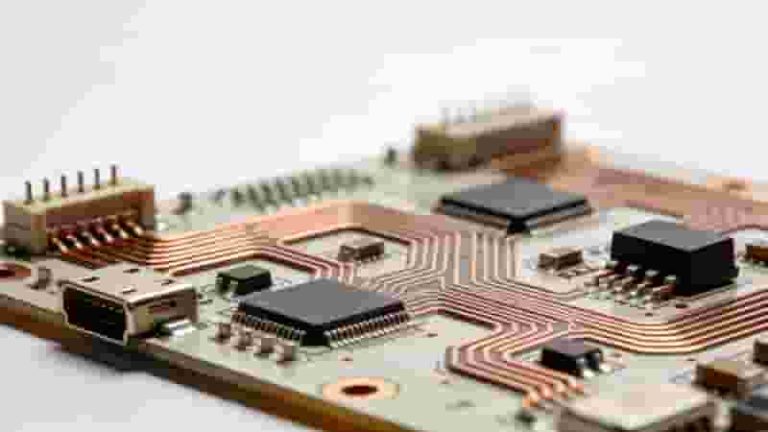
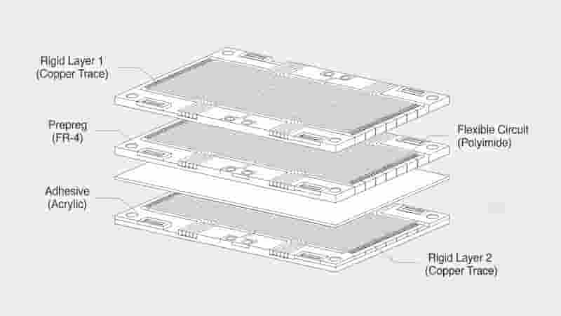
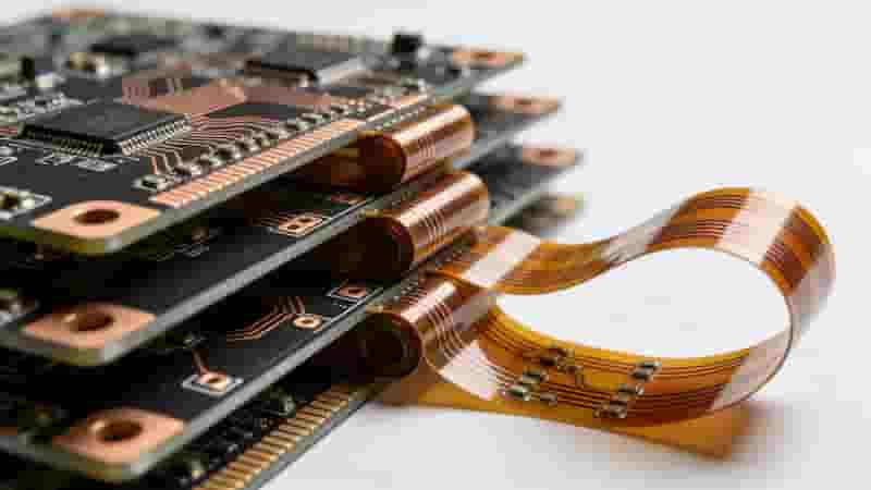
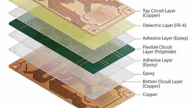
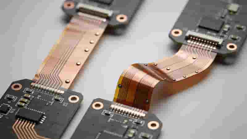
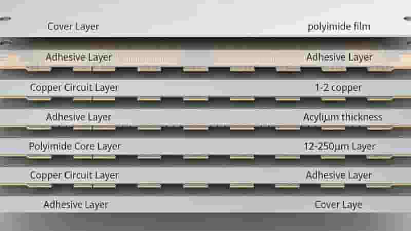
Rigid-Flex PCB Stackup defines the layered arrangement of conductive copper, flexible dielectric (polyimide), rigid core (FR4), adhesives and protective coatings in a single integrated circuit board. It combines rigid sections for component mounting and flexible sections for dynamic bending, folding and 3D assembly.
Key Features of Optimized Stackup
- Minimizes solder joints and connectors, improving long-term reliability
- Supports ultra-thin profiles and lightweight design
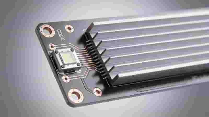
- Enhanced thermal dissipation for high-power devices
- Stable impedance control for high-speed and RF signals
- 3D routing capability to save assembly space
Common Types of Rigid-Flex Stackup
1. Single-sided rigid-flex stackup: Simple circuits, low-cost, wearable electronics
2. Double-sided rigid-flex stackup: Two conductive layers, moderate routing density
3. Multilayer Rigid-Flex PCB Stackup: 4L–12L+, used in aerospace, medical, 5G and automotive
Typical Layer Stackup Examples
4-Layer Rigid-Flex PCB Stackup
| Layer | Material | Function |
|---|---|---|
| Top Rigid Layer | FR4 | Component mounting |
| Flex Layer 1 | Polyimide | Signal routing |
| Flex Layer 2 | Polyimide | Signal routing |
| Bottom Rigid Layer | FR4 | Connector & support |
6-Layer Rigid-Flex PCB Stackup
Common configuration: 4 rigid layers + 2 flex layers or 2 rigid layers + 4 flex layers, supporting HDI, high-speed signals and high-density assembly.
Critical Design Considerations
• Bend radius: Min 8–10× flex thickness to avoid cracking
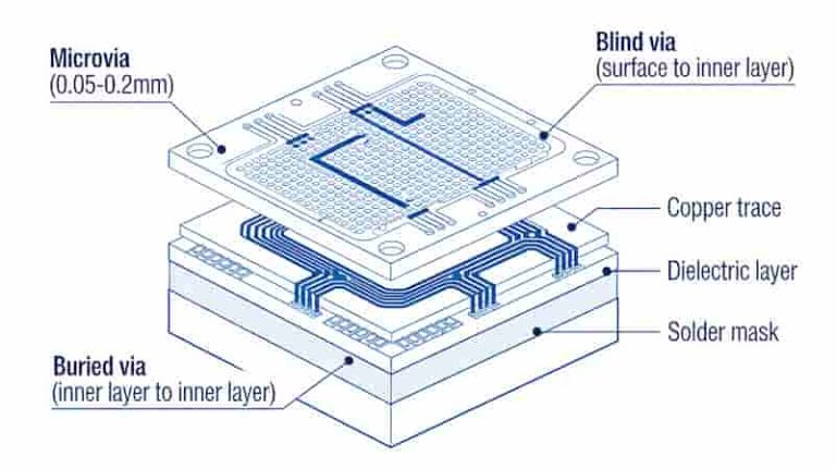
• Via design: Staggered vias in flex area to improve flexibility
• Impedance control: 50Ω / 75Ω / 90Ω / 100Ω for high-speed signals
• Coverlay & stiffener: Protect flex circuits and strengthen rigid areas
• DFM rules: Comply with IPC-6013, IPC-2221 and IPC-6018 standards
Material Selection Standards
Flex dielectric: Polyimide (PI), 25–50μm thickness
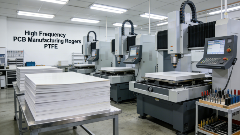
Rigid core: FR-4, High-Tg FR-4, Rogers for high frequency
Copper foil: 18–35μm standard, 70μm for high current
Surface finish: ENIG, Immersion Silver, HASL, Hard Gold
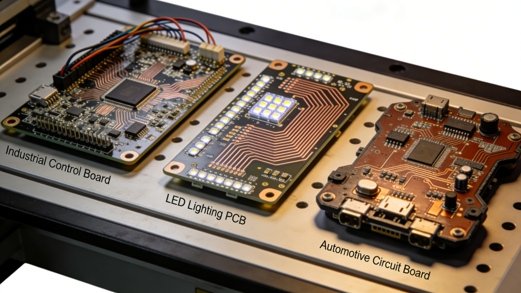
Industry Applications
• Medical: Implantable devices, monitors, surgical equipment
• Aerospace & defense: Satellites, drones, avionics
• Automotive: ADAS, EV controllers, infotainment
• 5G & IoT: Small base stations, foldable devices, sensors
• Consumer electronics: Foldable phones, wearables, cameras
Figure 5: Main applications supported by Rigid-Flex PCB Stackup
Summary
A well-designed Rigid-Flex PCB Stackup ensures flexibility, reliability, signal integrity and cost efficiency. It is essential for high-performance electronic products in medical, automotive, aerospace and 5G industries. Correct layer arrangement, material selection and DFM compliance directly determine production yield and long-term performance.
Get Your Custom Rigid-Flex PCB Stackup Solution
We provide professional rigid-flex PCB design, prototyping and mass production with optimized stackup, impedance control, DFM review and full testing. Send your Gerber or parameters for a free stackup proposal and quick quote.
Contact us today for:
- Free Rigid-Flex PCB Stackup evaluation
- Custom layer design & impedance simulation
- Prototype & mass production pricing
- Quick lead time & global delivery
Request Quote | Custom Stackup Design | Technical Support
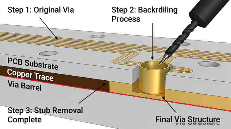
Backdrilling of Vias: The Definitive Guide for High-Speed PCB Signal Integrity
Standard PCB Thickness – The Complete Guide for Engineers & Buyers
Rapid PCB Prototyping | Accelerate Innovation & Speed Up Time-to-Market
Types of Flexible Circuit Boards: The Ultimate Guide to Flex PCBs
Copper Clad Laminate (CCL): The Complete 2026 Guide for PCB Manufacturing