We provide professional single layer PCB manufacturing with ISO-certified quality, fast lead times, cost-effective pricing and free DFM analysis for global industrial buyers, engineers and importers. Our single sided PCBs are widely used in LED lighting, power supplies, consumer electronics and industrial control equipment.
What Is a Single Layer PCB
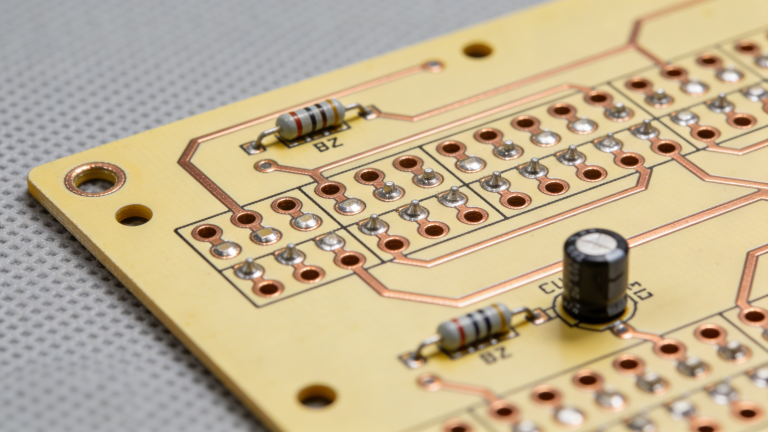
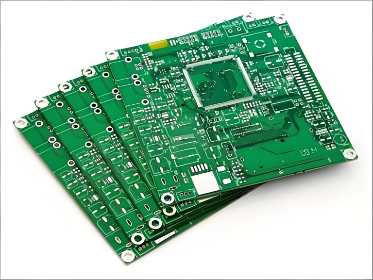
A single layer PCB (also named single sided PCB) is the most basic printed circuit board with only one conductive copper layer on an insulating substrate such as FR‑4, CEM‑1 or aluminum. All circuits, pads and components are mounted on one side, making it the most cost‑effective and easy‑to‑manufacture solution for simple circuit designs.
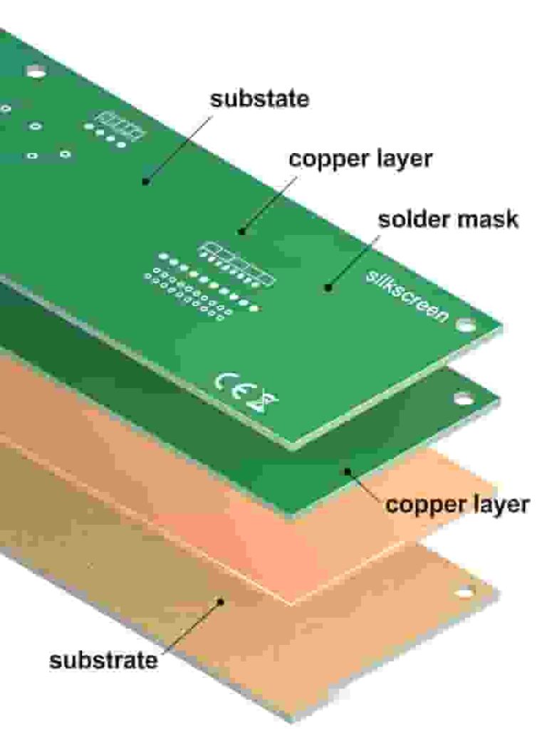
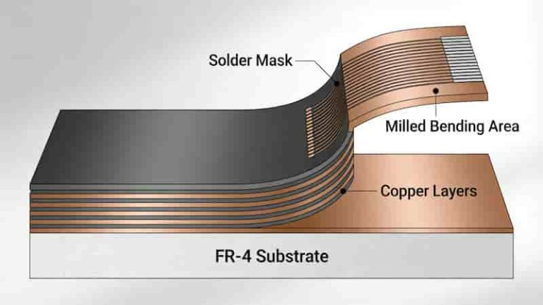
Single Layer PCB Basic Structure
Main Types of Single Layer PCBs
We support full customization for different single layer PCB types to meet various application requirements.
Single Layer Rigid PCB
Made of FR‑4 or CEM‑1 materials, the most widely used type for calculators, power supplies, controllers and household appliances.
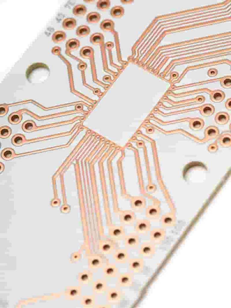
Single Layer Flexible PCB
Built with flexible polyimide materials, ideal for wearable devices, compact sensors and folding components.
Single Layer Rigid‑Flex PCB
Combines rigid and flexible substrates, used in compact cameras, medical devices and automotive sensors.
Single Layer High‑Frequency PCB
Uses high‑frequency materials like Rogers, designed for RF modules, communication equipment and signal transmission devices.
Single Layer Aluminum PCB
Features excellent thermal conductivity, perfect for high‑power LED lighting, drivers and heat‑dissipation equipment.
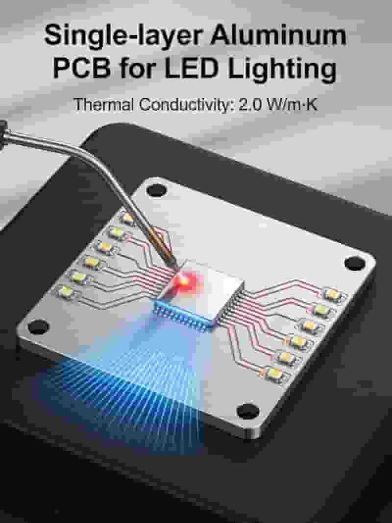
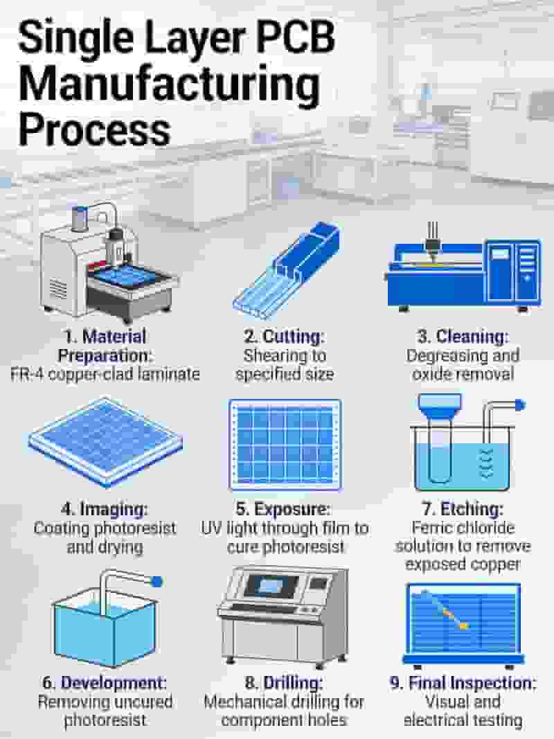
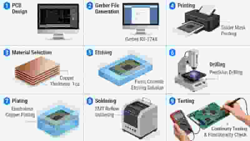
Single Layer PCB Manufacturing Process
Our standardized single layer PCB manufacturing follows IPC standards to ensure stable performance and high yield.
- Order Confirmation & DFM Check: Free design for manufacturability analysis to avoid production risks.
- Material Preparation: Select high‑quality base materials and copper foils.
- Circuit Printing & Etching: Transfer circuit patterns and remove excess copper accurately.
- Drilling: CNC drilling for component holes and mounting positions.
- Solder Mask & Silkscreen: Apply protective layer and print component labels.
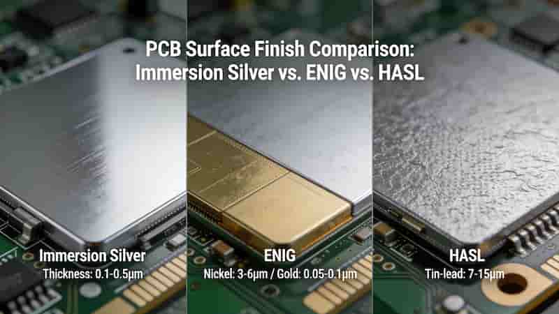
- Surface Finish: HASL, OSP, ENIG or other customizable finishes.
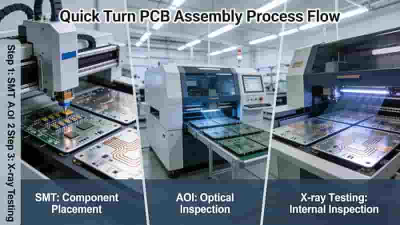
- Electrical Testing: AOI and flying probe test to ensure 100% electrical reliability.
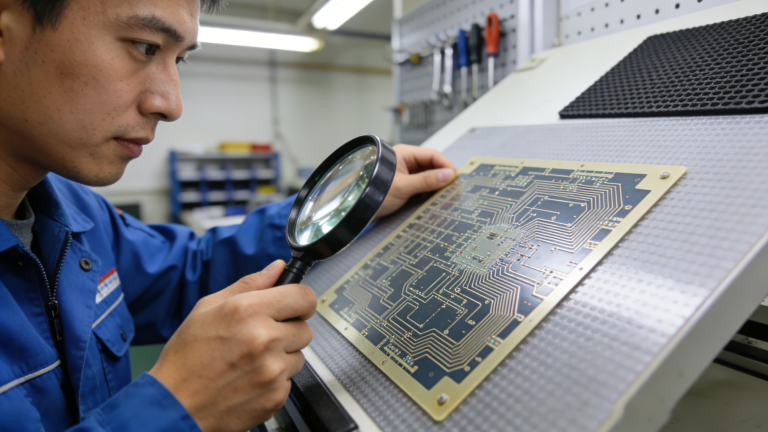
- Final Inspection & Packaging: Visual inspection and safe packaging for delivery.
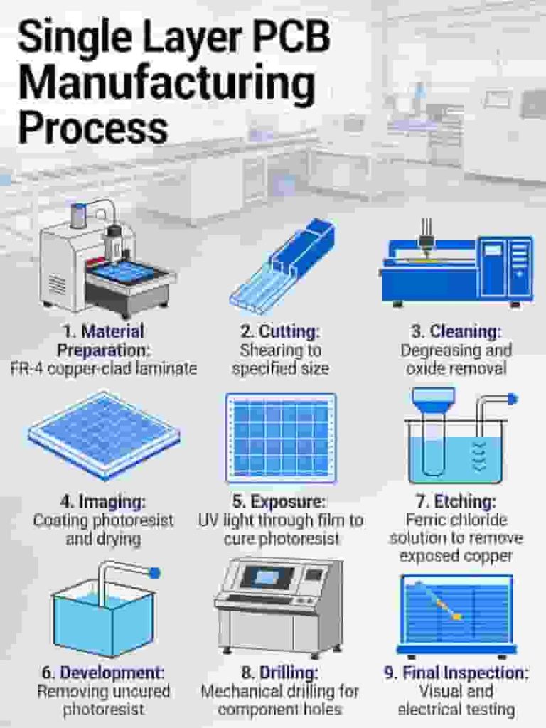
Single Layer PCB Full Manufacturing Flow
Key Benefits of Single Sided PCBs
Single layer PCB remains the top choice for low‑complexity projects due to its outstanding advantages:
- Cost‑Effective: Lowest production cost among all PCB types, ideal for mass production.
- Simplified Production: Shorter lead time and fewer manufacturing defects.
- High Reliability: Simple structure ensures stable performance and long service life.
- Easy Testing & Maintenance: Convenient electrical testing and repair work.
- Flexible Customization: Support various materials, sizes and surface finishes.
Single vs Double vs Multilayer PCBs
| Feature | Single Layer PCB | Double Layer PCB | Multilayer PCB |
|---|---|---|---|
| Conductive Layers | 1 | 2 | 3 or more |
| Cost | Lowest | Moderate | High |
| Complexity | Simple | Moderate | High |
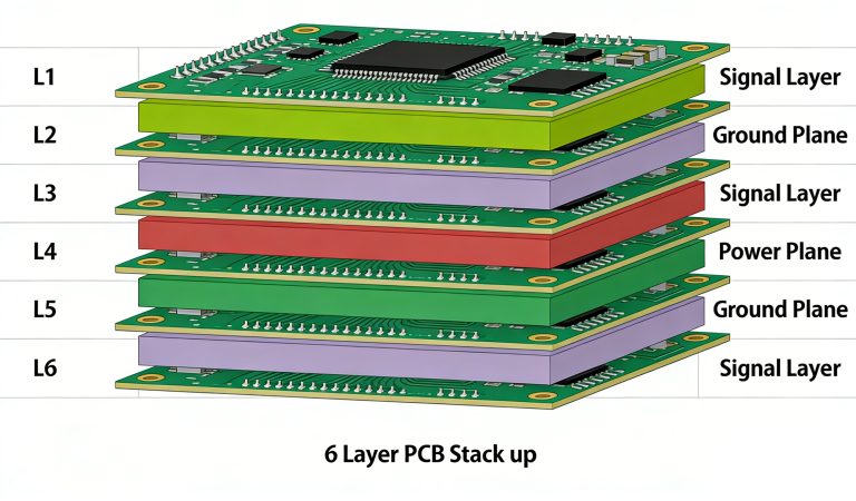
| Typical Applications | LED, power supplies, calculators | Consumer electronics, controls | Aerospace, medical, automotive |
Standard Technical Specifications
We provide stable and customizable parameters for single layer PCB manufacturing:
- Base Materials: FR‑4, CEM‑1, Aluminum, PI
- Copper Thickness: 0.5oz – 2oz
- Board Thickness: 0.4mm – 3.0mm
- Minimum Trace Width: 0.2mm
- Minimum Hole Size: 0.3mm
- Surface Finish: HASL, OSP, ENIG, Immersion Tin
- Testing: AOI, Flying Probe, Impedance Test
Conclusion
Single layer PCB is the most economical and practical solution for simple circuit applications. With professional single layer PCB manufacturing, stable quality control, fast delivery and competitive pricing, we help global customers optimize costs and improve product reliability.
Request a Free Quote Now
Get professional single sided PCB solutions with free DFM check, fast prototyping and competitive pricing. Send your Gerber files now to receive a detailed quote within 24 hours.
Get My Free Quote
We support mass production and rapid prototyping for single layer PCB projects worldwide. Contact us today for your customized PCB solutions.
Immersion Silver PCB Surface Finish: Benefits, Applications, Cost Analysis & IPC Standards
Via-in-Pad for Printed Circuit Boards: Complete Technical Guide
Microvias in PCBs: Complete Technical Guide for HDI & Miniaturization
What is a PCB Manufacturer? The Definitive Guide
Semi-Flex PCBs: The Ultimate Bridge Between Rigid and Flex PCBs