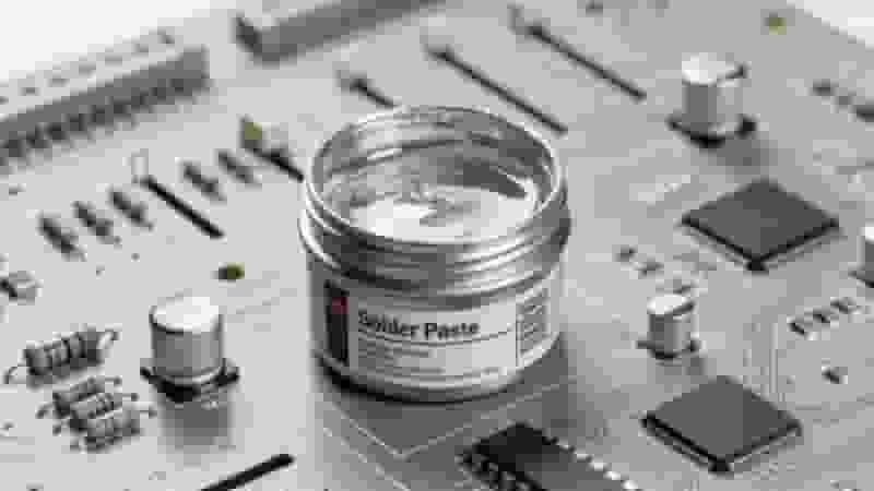
Solder paste is the foundational material for assembly manufacturer in China, enabling reliable electrical and mechanical connections between components and PCB pads. This professional guide covers definition, composition, types, storage, printing process, inspection, and best practices for industrial buyers and engineers.
What Is Solder Paste in SMT PCB Assembly?
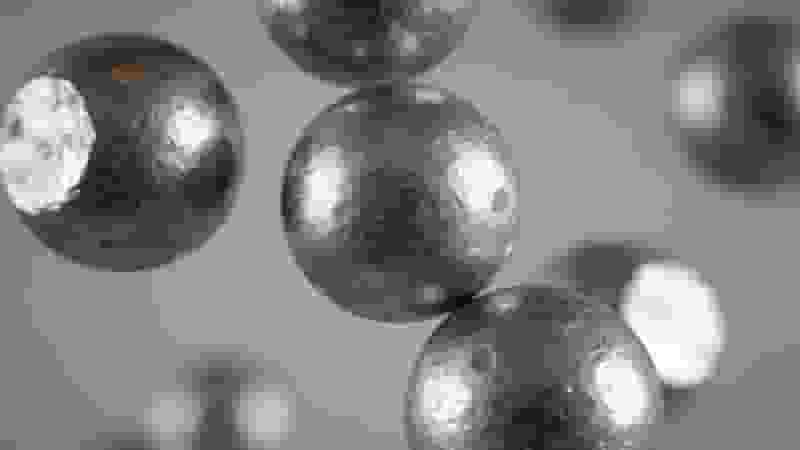
Solder paste is a thixotropic composite material used in SMT PCB assembly. It consists of microscopic solder alloy powder, flux, and additives, providing temporary adhesion for components and forming permanent solder joints during reflow soldering.
As the most critical material in surface mount technology, solder paste directly determines the reliability, yield, and performance of PCB assembly. Industry statistics show 60–70% of SMT defects originate from improper solder paste selection or printing control.
Main Components of Solder Paste
High-quality solder paste for PCB assembly contains four core components:
- Flux: Removes oxides from PCB pads and component pins, reduces surface tension, and improves wetting
- Solder Powder: Lead-free alloys (Sn96.5/Ag3.0/Cu0.5) for RoHS-compliant PCB assembly
- Resin: Enhances adhesion and protects solder joints from re-oxidation
- Solvent: Adjusts viscosity and ensures smooth printing performance
Types & Grades of Solder Paste
Solder paste is classified by alloy type, melting point, and particle size (IPC standards) to match different PCB assembly requirements:
- Lead-free vs. Lead-containing: Modern SMT PCB assembly primarily uses lead-free solder paste for environmental compliance
- Melting Point: High-temperature (≥217°C) for reliable industrial PCB applications
- Particle Size (IPC Type): Type 3–5 for fine-pitch components in high-density PCB assembly
| IPC Type | Particle Size (μm) | Best For PCB Assembly |
|---|---|---|
| Type 3 | 25–45 | Standard SMT PCB assembly |
| Type 4 | 20–38 | Fine-pitch PCB components |
| Type 5 | 10–25 | High-density PCB assembly |
Solder Paste Storage & Handling
Proper storage preserves solder paste performance and ensures stable PCB assembly quality:
- Storage temperature: 2–10°C (refrigerated, not frozen)
- Shelf life: 3–6 months sealed; use within 24 hours after opening
- Thaw at room temperature for 4–6 hours before use; avoid condensation
- Stir uniformly to restore consistent viscosity for solder paste printing
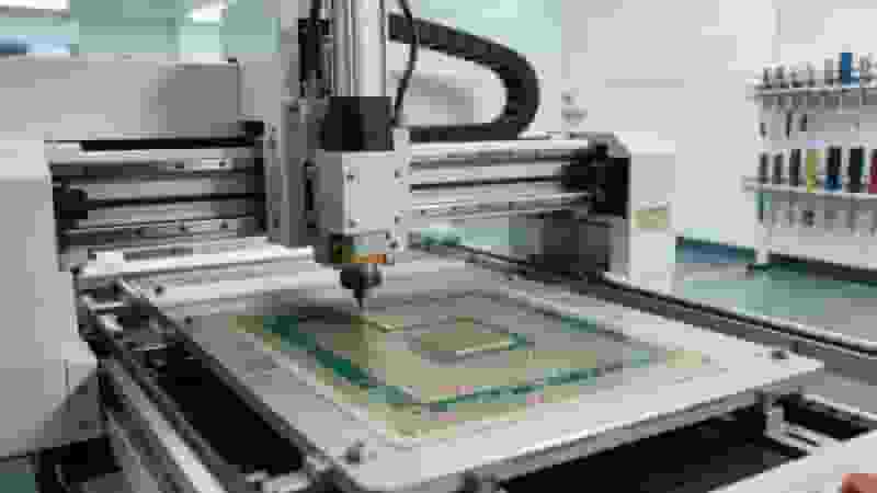
Solder Paste Printing Core Process
Solder paste printing is the first and most critical step in SMT PCB assembly:
- Stencil Alignment: Precision alignment between SMT stencil and PCB
- Paste Application: Squeegee pushes solder paste through stencil apertures
- Stencil Separation: Controlled lift-off to maintain paste shape on PCB pads
- Pre-Inspection: Visual or SPI check before component placement
Key Parameters for Stable Solder Paste Printing
Optimal parameters ensure consistent solder paste transfer in PCB assembly:
- Squeegee angle: 45–60° for best paste roll
- Print speed: 20–50 mm/s based on PCB pad size
- Pressure: Sufficient to clean stencil without damaging PCB
- Separation speed: 0.1–0.5 mm/s to prevent bridging
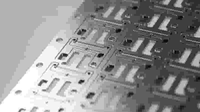
SMT Stencil for Precision PCB Assembly
SMT stencils (stainless steel, laser-cut) control solder paste volume and position on PCB:
- Standard thickness: 0.12 mm for general PCB assembly; 0.15 mm for larger pads
- Aperture design: Match PCB pad size to prevent insufficient or excess paste
- Maintenance: Regular cleaning to avoid clogging and ensure consistent solder paste printing
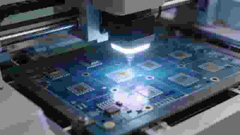
Solder Paste Inspection (SPI)
3D SPI (Solder Paste Inspection) ensures solder paste printing quality in SMT PCB assembly by measuring:
- Paste height, area, and volume on PCB pads
- Alignment accuracy (offset from PCB design)
- Defects: Bridging, insufficient paste, or smearing
Early detection reduces rework and ensures high-yield PCB assembly.
Solder Paste Type Comparison for PCB Assembly
| Feature | Lead-Free Solder Paste | Lead-Containing Solder Paste |
|---|---|---|
| Compliance | RoHS, EU, global PCB standards | Limited to special applications |
| Melting Point | 217–220°C | 183°C |
| PCB Assembly Use | Industrial, medical, consumer PCB | Legacy, non-critical products |
Summary
Solder paste and solder paste printing are foundational to high-quality SMT PCB assembly. Proper material selection, storage, process control, and inspection directly impact PCB reliability, yield, and cost efficiency.
For industrial buyers and engineers, partnering with experienced PCB assembly providers ensures optimized solder paste usage and consistent, high-performance PCB products.
Need Professional SMT PCB Assembly Service?
We provide high-quality, cost-effective PCB manufacturing and SMT assembly with strict solder paste control and IPC standards.
Request a Quote | Custom PCB Solution
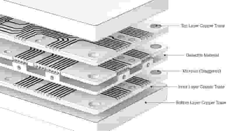
The Essentials of Microvias – Enabling Miniaturization in PCBs
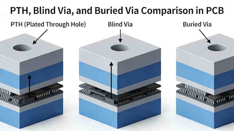
Blind Vias & Buried Vias in PCBs – The Complete Technical Guide
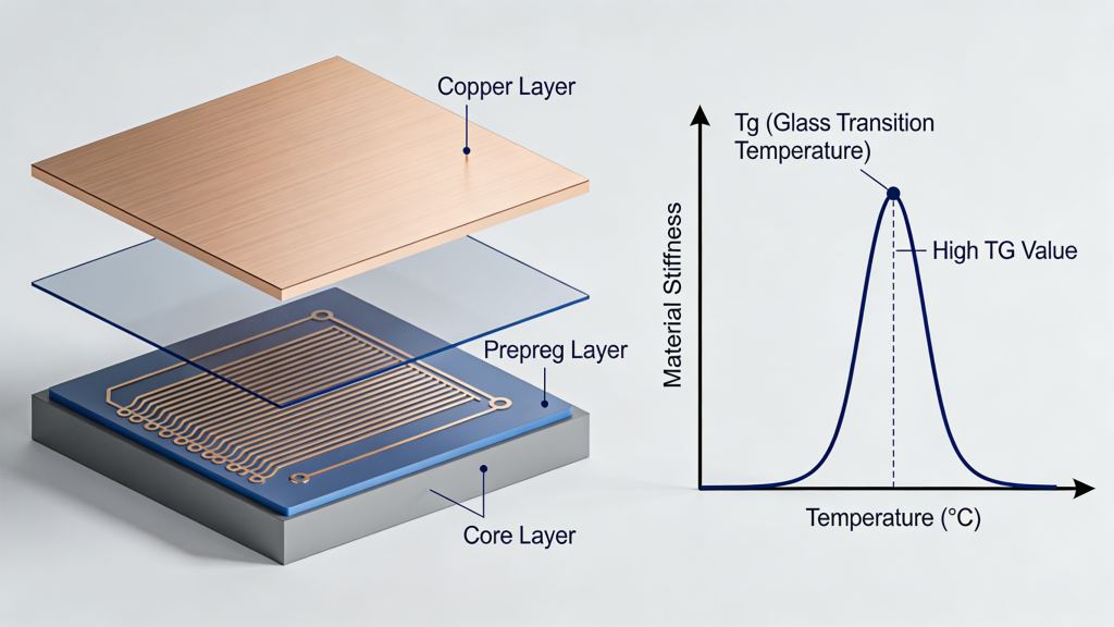
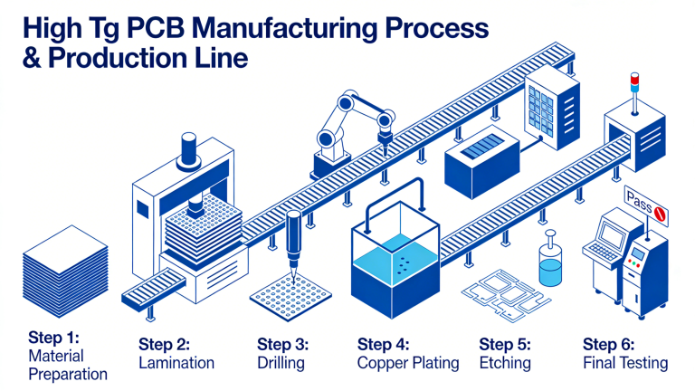
High TG PCB Material: Thermal Stability, Key Benefits, Industrial Applications & Professional Fabrication Solutions
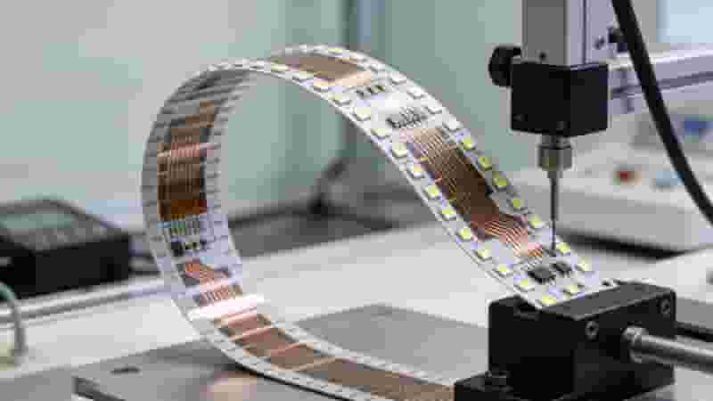
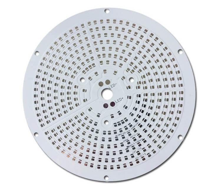
Professional LED PCB Manufacturing & Assembly Services
Quick Turn PCB Assembly in USA: The Strategic Guide to Speed, Cost & Reliability