|

What Is PCB OSP Surface Finish? A Comprehensive Guide

OSP PCB Production Line Coating Process

OSP (Organic Solderability Preservative) is a lead‑free, water‑based organic coating applied to exposed copper pads on printed circuit boards to prevent oxidation and ensure reliable soldering for SMT assembly. This complete guide covers definition, process, pros & cons, comparisons, storage, assembly best practices, and ideal applications for global engineers and buyers.

What Is PCB Surface Finish?

A PCB surface finish is a protective layer applied after solder mask to shield exposed copper traces from oxidation and provide a solderable surface for component mounting. It directly impacts board reliability, assembly yield, cost, and compliance with RoHS and WEEE standards.

Key functions:

  • Protect copper from oxidation and corrosion
  • Ensure strong and stable solder joints
  • Support fine‑pitch and high‑density SMT assembly
PCB Surface Finish Overview Copper Protection SMT Assembly

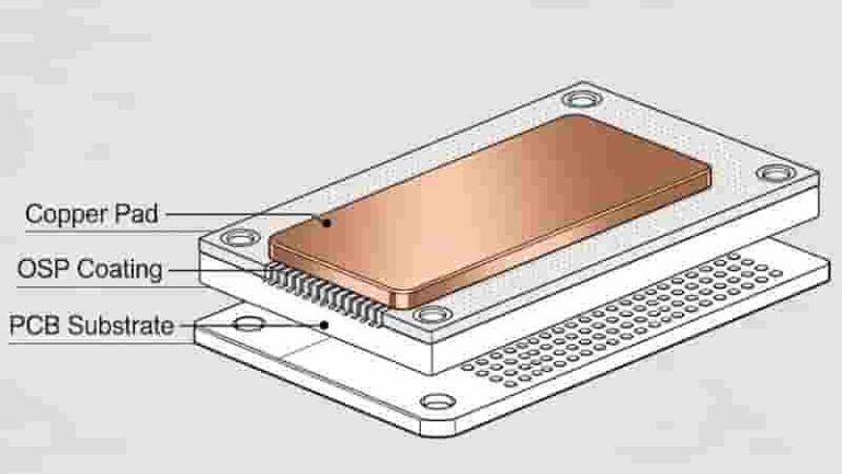
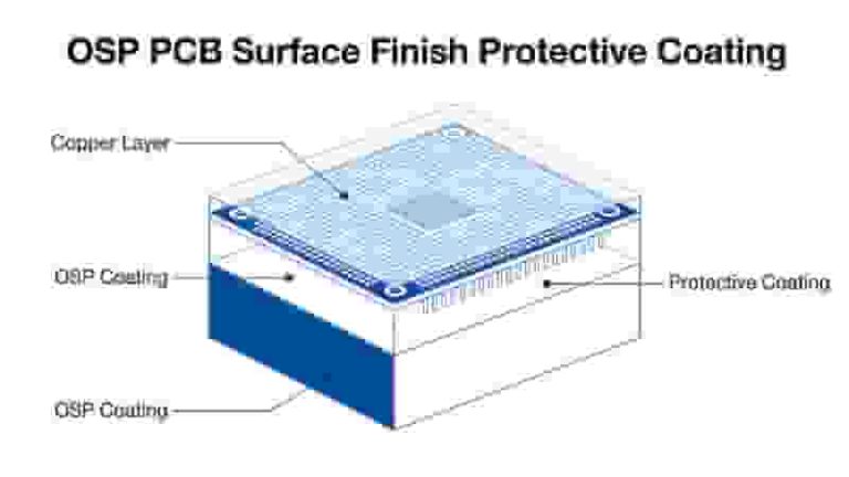
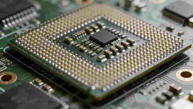
What Is OSP Surface Finish?

OSP (Organic Solderability Preservative) is a transparent, water‑based organic coating that bonds to copper surfaces. It is one of the most cost‑effective and eco‑friendly lead‑free surface finishes widely used in consumer electronics, automotive, industrial, and telecommunication devices.

Unlike metallic finishes, OSP is thin, flat, and ideal for fine‑pitch components, BGAs, and lead‑free reflow soldering.

PCB OSP Coating Structure Transparent Copper Protection

OSP Surface Finish Manufacturing Process

The OSP application process ensures uniform coverage and strong adhesion to copper pads:

  1. Cleaning: Remove contaminants, grease, and oxides
  2. Micro‑etching: Roughen copper for better bonding
  3. DI rinsing: Eliminate residual ions
  4. OSP coating: Apply organic film at pH 4.0–7.0
  5. Drying: Cure and stabilize the protective layer
OSP PCB Production Line Coating Process

Advantages & Disadvantages of OSP Surface Finish

Advantages

  • Excellent flatness for fine‑pitch and BGA components
  • Lowest cost among common surface finishes
  • RoHS and WEEE compliant, eco‑friendly
  • Simplified manufacturing and fast processing
  • Good solderability for lead‑free assembly

Disadvantages

  • Shorter shelf life: 6–12 months
  • Sensitive to handling, moisture, and thermal cycles
  • Difficult visual inspection due to transparency
  • Limited reflow cycle tolerance
Fine Pitch BGA OSP PCB Flat Surface

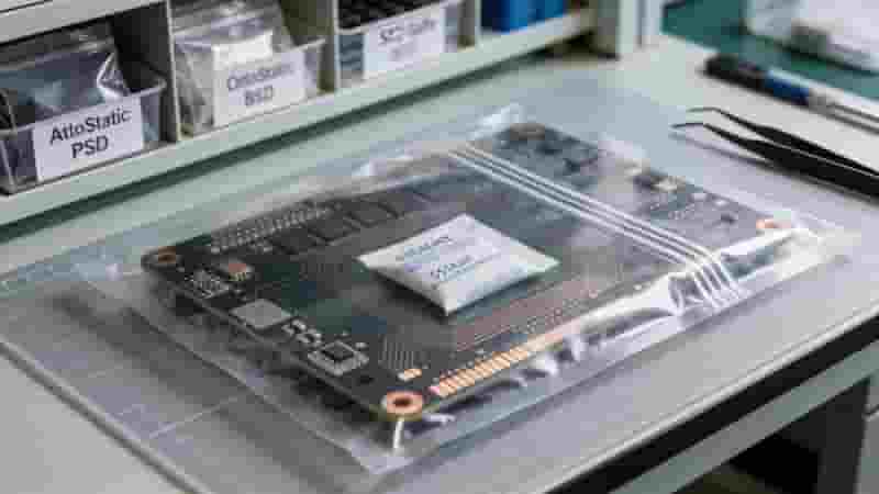
OSP PCB Storage & Assembly Guidelines

Storage Conditions:

  • Vacuum packaging with desiccants
  • Temperature: 15–30°C
  • Humidity: 30–70% RH
  • Avoid direct sunlight and excessive heat

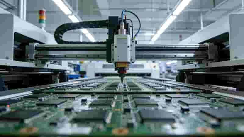
Assembly Best Practices:

  • Minimize exposure to open air
  • Avoid repeated high‑temperature reflow
  • Use proper handling with gloves
  • Optimize solder paste and stencil design

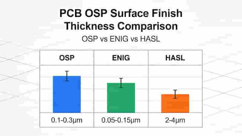
OSP vs Other PCB Surface Finishes

FeatureOSPENIGImmersion SilverLead‑Free HASL
CostLowHighModerateModerate
FlatnessExcellentGoodGoodPoor
Shelf Life6–12 months12+ months6–12 months12+ months
RoHS CompliantYesYesYesYes
OSP vs ENIG vs HASL PCB Surface Finish Comparison

Conclusion

OSP surface finish is a top choice for cost‑sensitive, high‑volume, lead‑free PCB applications requiring excellent flatness and environmental compliance. It delivers reliable performance for consumer electronics, automotive, industrial, and telecommunication devices when properly stored and assembled.

Understanding its process, strengths, and limitations helps you select the best surface finish for your PCB design and production needs.

Need Professional OSP PCB Manufacturing?

Get high‑quality OSP finished PCBs, quick quotes, DFM analysis, and reliable global delivery for your industrial and commercial projects.

Request a Free Quote

Low Volume PCB Assembly Overview SMT Small Batch Production

Low-Volume & Small Batch PCB Assembly Service 

Posted on
0 Comments
Low-volume or small-batch PCB assembly is your best solution for flexible assembly parts on a relatively small batch of bare PCB boards! A low-cost PCB prototype is essential if you are looking at a new launch. After all, you do not want a situation where you deal with errors after a high-volume or mass production run. Alternatively, you could be…
When to use via-in-pad in PCB for BGA and fine-pitch components

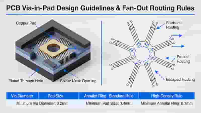
Via-In-Pad Design Guidelines and Manufacturing Process for PCB

Posted on
0 Comments
Via-in-pad (VIP) is a critical PCB design technique where vias are drilled directly on SMD and BGA pads to support high-density interconnects. This guide covers via-in-pad fundamentals, design rules, manufacturing processes, and comparisons between VIP and non-VIP processes to ensure reliable PCB assembly and performance. What Is Via-In-Pad? Via-in-pad (VIP) means drilling vias directly on…
Via-in-Pad Cross Section PCB HDI Technology

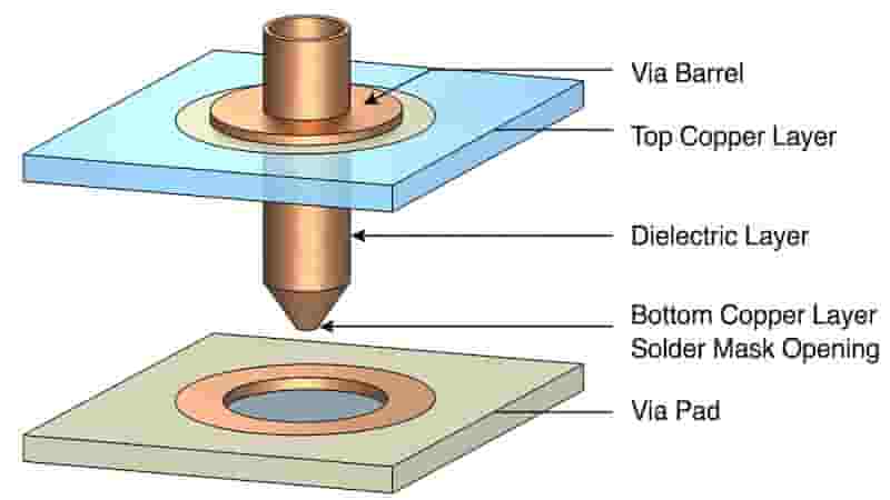
Via-in-Pad for Printed Circuit Boards: Complete Technical Guide

Posted on
0 Comments
Via-in-Pad technology places vias directly within surface mount pads to save space, improve routing efficiency, and enhance PCB density for HDI and high-speed designs. What Is Via-in-Pad Technology for PCBs? Before understanding via-in-pad, let’s review common PCB via types: Plated-through holes (PTHs) span the entire board, blind/buried vias connect partial layers, and microvias (~0.1mm) link…
PCB Solder Mask full color options green red blue white black matte

PCB Solder Mask: The Complete Technical Guide for Global Buyers

Posted on
0 Comments
PCB Solder Mask (also known as solder resist) is a protective polymer layer applied to printed circuit boards to prevent solder bridging, resist oxidation, improve insulation, and ensure long‑term reliability in SMT assembly and industrial applications. This guide covers definitions, types, colors, processes, DFM rules, IPC standards, testing, and troubleshooting for engineering and procurement teams…
Automotive Printed Circuit Boards Structure and Basics

Automotive Printed Circuit Boards: Reliable Solutions for Vehicle Electronics

Posted on
0 Comments
Automotive printed circuit boards are critical building blocks for modern vehicles, supporting engine control, infotainment, safety systems, ADAS, and electric powertrains. These boards deliver stable performance under extreme temperatures, vibration, humidity, and EMI while meeting strict automotive quality standards. What Are Automotive PCBs? Automotive printed circuit boards are specially designed and manufactured for vehicle electronic…
Rigid PCB Prototype FR-4 Industrial Circuit Board

Learn the Essential Requirements for PCB Prototype Manufacturing in 2025

Posted on
0 Comments
Summary: Master critical standards for PCB prototype manufacturing including file formats, design rules, layer stackup, and documentation. Optimize your prototyping workflow with expert best practices to achieve high-quality, cost-effective, and on-time PCB prototypes for industrial and engineering applications. Prototype PCB Fabrication PCB prototyping is a crucial step in the electronics design process, enabling designers to…

FAQs About OSP PCB Organic Solderability Preservative Finish

A: OSP is eco-friendly water-based transparent organic coating covered on bare copper pads to stop oxidation and secure good solderability for SMT and BGA assembly.

A: Low production cost, ultra-flat pad surface for fine-pitch BGA, fully RoHS/WEEE compliant and high efficiency during manufacturing.

A: Short shelf life only 6–12 months, vulnerable to high temperature & humid air, invisible coating brings difficulty for visual inspection.

A: Vacuum sealed with desiccant, store at 15~30°C & 30%~70%RH, stay away from sunlight and high-temperature environment.

A: Reduce bare-air exposure time, limit repeated reflow cycles, wear gloves during handling and customize matched solder paste parameters.

A: OSP lowest cost & best flatness but short shelf life; ENIG high cost with long storage; HASL low cost yet uneven pad surface.

A: Large-volume consumer electronics, communication products, cost-controlled automotive modules and regular industrial control circuit boards.

A: Low unit cost, outstanding flatness matching fine-pitch stencil printing and eco compliance to satisfy global large-batch lead-free production demand.

Similar Posts