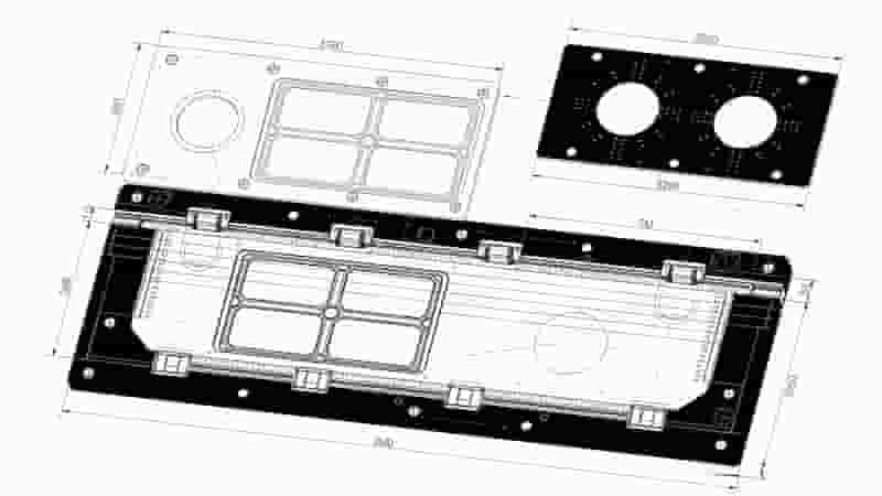
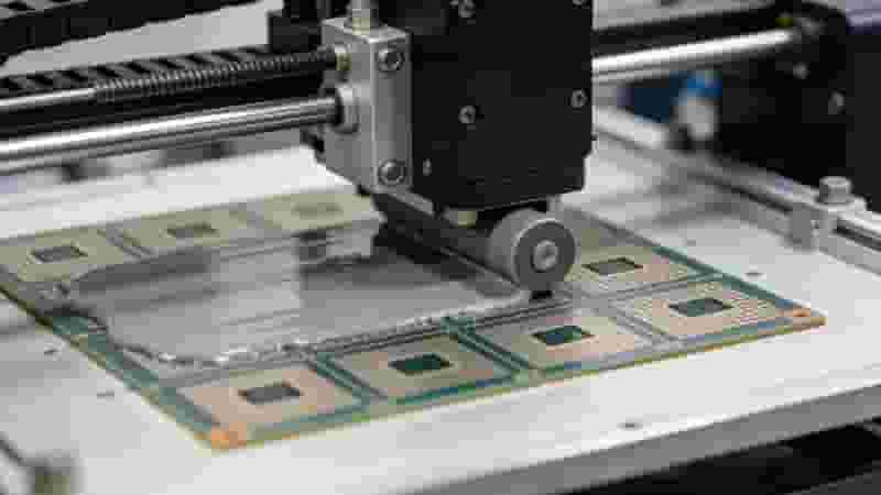
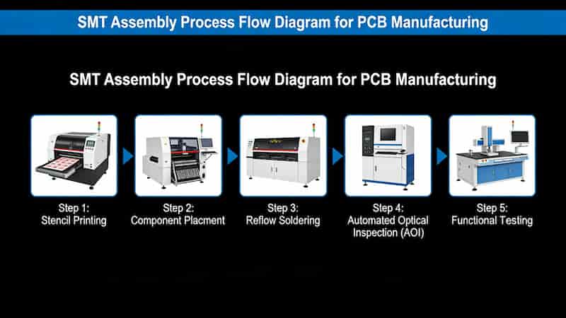
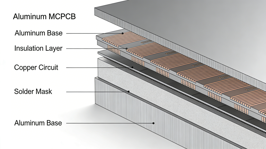
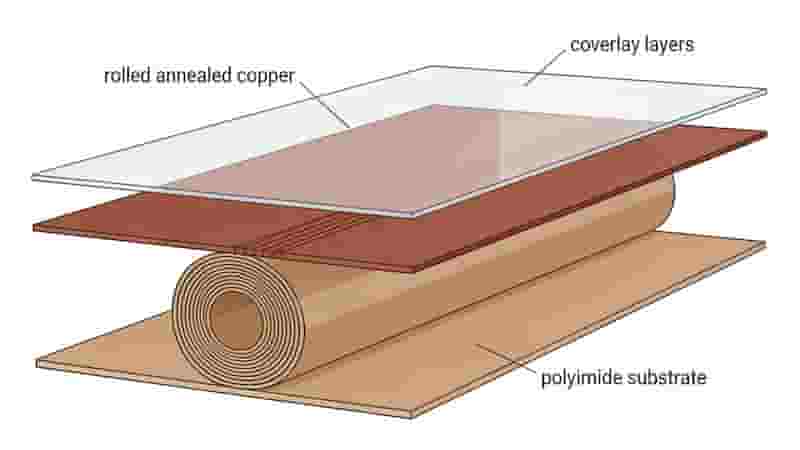
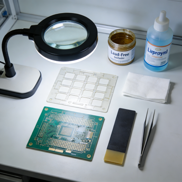
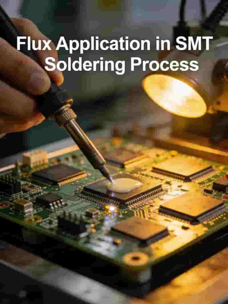
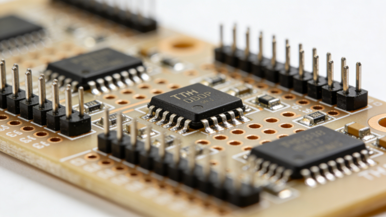
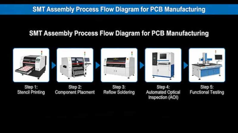
Step Stencil Manufacturing provides precision-engineered multi-level thickness stencils for advanced PCB assembly, delivering controlled solder paste deposition for mixed-component boards and high-yield SMT production.
What Is a Step Stencil
A Step Stencil (multi-level stencil) is a precision SMT assembly tool designed to apply controlled solder paste volumes to PCB surfaces. Unlike standard uniform-thickness stencils, step stencils feature engineered thickness variations to support both fine-pitch components (0201, 0402, QFP) and larger components (BGA, connectors) on a single board.
This specialized design eliminates solder bridging, insufficient joints, and paste smearing, directly improving assembly quality and production yield for modern high-density PCB assembly.
Types of Step Stencils
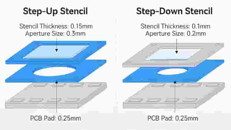
Step-Up Stencil
Thicker localized zones deliver increased solder paste volume for large components, power connectors, and high-current pads.
Step-Down Stencil
Thinner localized zones prevent excessive paste for fine-pitch chips, micro-components, and densely packed areas.
Multi-Level Step Stencil
Combines multiple thickness profiles for complex PCB layouts with mixed component types and sizes.
Key Benefits of Step Stencils
Precise solder paste volume control reduces assembly defects by up to 70%
Single-stencil solution replaces multiple standard stencils, simplifying production
Enhanced paste release efficiency ensures consistent prints across complex layouts
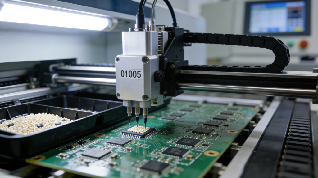
Supports 01005, 0201, µBGA, and advanced fine-pitch components
Lowers rework costs and improves overall production efficiency
Industry Applications
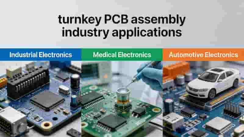
Step Stencil Manufacturing supports high-reliability PCB assembly across critical industries:
Consumer Electronics: Smartphones, wearables, IoT devices with dense mixed components
Automotive Electronics: ECUs, sensors, infotainment systems for harsh environments
Medical Devices: Diagnostic equipment, implants requiring zero-defect assembly
Telecommunications: 5G infrastructure, routers, high-speed data equipment
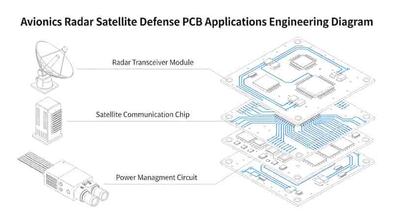
Aerospace & Defense: Avionics, satellite systems with mission-critical PCBs
Our Step Stencil Manufacturing Process
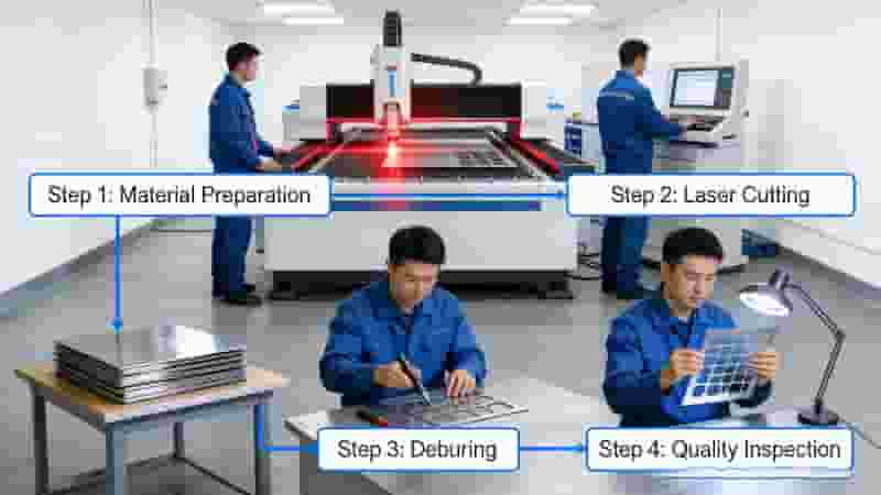
Design & DFM Analysis: Review Gerber data to optimize step positions and thickness
Material Preparation: High-tensile stainless steel foil with stress relief
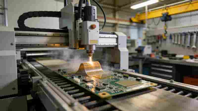
Precision Fabrication: Laser cutting, micro-machining, or photo-chemical etching
Step Forming: Laser welding or chemical etching for multi-level structures
Surface Treatment: Electropolishing or nano-coating for better paste release
Quality Inspection: 3D profilometry and optical verification for ±0.025mm accuracy
Why Choose Our Step Stencil Manufacturing
Advanced laser systems with ±0.025mm positional accuracy
Custom thickness profiles (0.1mm–0.2mm) for any PCB design
Optional nano-coating and electropolishing for extended life
ISO 9001 & RoHS compliant, full quality inspection
Fast turnaround: prototypes in 3–7 days, global express shipping
Expert engineering support for DFM and stencil optimization
Step Stencil vs Standard Stencil
Feature
Step Stencil
Standard Stencil
Thickness
Multi-level variable
Single uniform
Best For
Mixed fine-pitch & large components
Uniform component sizes
Defect Rate
Very low
Higher on mixed boards
Assembly Yield
Significantly improved
Standard performance
Summary
Step Stencil Manufacturing delivers precision multi-level SMT stencils engineered for modern PCB assembly challenges. Our custom step stencils provide accurate solder paste control, reduce defects, streamline production, and support high-yield manufacturing for global electronics industries.
Get Your Custom Step Stencil Quote
Request a free quote, technical consultation, or prototype stencil for your PCB assembly project.
Custom LED grow light PCB solutions with high-thermal aluminum substrates, full-spectrum design support, and turnkey PCB assembly for commercial indoor farming, greenhouses, and horticultural lighting systems. What Are LED Grow Lights? LED grow lights are artificial lighting systems engineered to emit optimized light spectra for plant photosynthesis. They replace or supplement natural sunlight for indoor…
Multilayer PCB stackup and thickness design directly determines signal integrity, EMC performance, impedance control and mechanical reliability of high-speed electronic products. This guide covers standard stackup structures, typical thickness values, and professional selection tips from 4-layer to 14-layer PCBs for industrial and export-grade applications. Why Multilayer PCB Stackup And Thickness Matter In modern electronics, products…
This professional guide explains PCB stencil usage for SMT assembly, including preparation, alignment, printing, inspection, cleaning, maintenance and best practices to ensure high-quality solder paste deposition for prototypes and mass production. What is PCB Stencil Stencils, also known as SMT stencil, are specialized molds for SMT assembly. Their primary function is to assist solder paste…
Copper Core PCB delivers superior thermal conductivity and stability for high-power electronics, while Metal Core PCB offers cost-effective thermal management for general industrial and commercial applications. Introduction to PCB Technology Printed Circuit Boards (PCBs) are the foundational building blocks of modern electronic devices. From consumer electronics to industrial machinery, PCBs ensure reliable electrical connectivity and…
The SMT PCB assembly process is the core of modern electronics manufacturing. This guide walks you through each step, from barcode printing to final inspection, ensuring high reliability and efficiency for your PCBs. Introduction to SMT PCB Assembly Surface-mount technology (SMT) stands as the foundation of modern electronics manufacturing, supporting the production of compact, high-performance devices including…
UK PCB prototype manufacturing delivers rapid, reliable printed circuit board prototypes for engineers, procurement teams, and industrial buyers. We provide fast lead times, competitive pricing, and consistent quality compliant with IPC, ISO 9001, RoHS, and REACH standards to support UK and global electronics development. PCB Prototype Capabilities & Specifications Our UK PCB prototype manufacturing supports…
Summary: This professional guide covers PCB vias definitions, core types, structure, design rules, aspect ratio, annular ring, manufacturing processes, and reliability standards. It helps engineers and buyers select the right via solutions for multilayer, high-speed, and HDI PCBs to ensure signal integrity, yield, and cost efficiency. What Are PCB Vias A via is a vertical…
Explore the complete evolution of printed circuit boards from early electromagnetic theory to modern HDI, flexible, and optical PCBs. This timeline covers key inventions, military adoption, mass commercialization, and future trends for global electronics manufacturing. PCB Prehistoric Era & Electromagnetic Foundations The journey of printed circuit boards starts with the discovery of electromagnetic principles that…
PCB prototyping is a vital step in electronics manufacturing, ensuring reliable mass production by validating circuit designs, minimizing defects, and optimizing costs. From multilayer to single-sided boards, prototyping enhances quality and efficiency. Explore the key benefits and best practices for selecting a trusted PCB prototype manufacturer. Introduction Printed Circuit Boards (PCBs) are the backbone of…
Plated Through Holes (PTH) are the foundation of reliable multilayer PCB connectivity. This guide covers PTH design, manufacturing, IPC standards, quality control, and best practices for industrial buyers and engineers. What Are Plated Through Holes (PTH) in PCBs? A Plated Through Hole (PTH) is a drilled hole through the PCB substrate with a continuous copper…
Flexible circuit board materials directly define flexibility, thermal stability, electrical performance, and reliability of FPCs. This professional guide covers substrates, conductors, adhesives, protective layers, stiffeners, and selection standards for global industrial buyers, engineers, and procurement teams. What Are Flexible Circuit Boards A flexible circuit board (FPC) is a lightweight, bendable circuit built on flexible insulating…
Learn professional flex PCB soldering techniques, temperature control, defect prevention, and step-by-step processes to ensure reliable, long-lasting assemblies for industrial and electronic applications. Why Flex PCB Soldering Is Different From Rigid PCBs Flex PCBs use thin polyimide substrates that are highly sensitive to heat and mechanical stress. While basic solder principles match rigid boards, flex…
As a dedicated high frequency PCB manufacturer, we provide reliable RF and microwave circuit boards from 500 MHz up to 20 GHz, using Rogers, PTFE and hybrid stackups to ensure stable signal integrity and low loss. High Frequency PCB Services We Provide As an experienced high frequency PCB manufacturer, we offer complete RF and microwave…
We specialize in LED PCB manufacturing and assembly with aluminum, copper & flexible substrates featuring superior heat dissipation. ISO 9001 certified, fast turnaround & competitive pricing for global LED lighting projects. Superior Heat Dissipation 1-9 W/mK thermal conductivity Fast Turnaround 24-hour quote, 3-5 days delivery ISO 9001 Certified International quality standard One-Stop PCBA Service From…
Understanding flexible PCB costs is essential for engineers, procurement teams, and manufacturers looking to control budgets while maintaining quality. This guide breaks down 16 critical factors that shape FPC pricing in 2025, including materials, layer count, manufacturing processes, order volume, and lead time. We also share practical cost‑saving strategies to help you optimize your next…
We provide end-to-end turnkey PCB assembly supporting full and partial models, with SMT assembly, THT, BGA/QFN, rigorous testing, and global logistics for industrial buyers, engineers, and importers. What Is Turnkey PCB Assembly Turnkey PCB assembly is a one-stop manufacturing solution covering PCB fabrication, component sourcing, assembly, testing, and delivery. We manage the full supply chain…
SMT (Surface Mount Technology) and SMD (Surface Mount Device) are core concepts in PCB assembly. SMT is the automated assembly process for mounting components onto PCBs, while SMD refers to the miniaturized components used in this process. This guide clarifies their definitions, differences, workflow, and applications for global engineers and buyers. Introduction In the fast-evolving…
Standard PCB thickness is critical for mechanical strength, signal integrity, and assembly compatibility. This guide covers definitions, industry standards, influencing factors, manufacturing constraints, and design best practices for global industrial buyers. What Is Standard PCB Thickness The global standard PCB thickness is 1.57 mm (0.062 in), commonly referenced as 1.6 mm for simplicity. This is…
We specialize in high‑reliability PCB manufacturing and assembly for aerospace and defense electronics. Our mission‑critical circuit boards meet IPC Class 3, Mil‑Spec, and AS9100 standards for extreme environments, avionics, satellites, radar, and defense systems. Critical Aerospace & Defense PCB Applications Our PCB manufacturing and assembly supports mission‑critical electronics across aviation, space, land, and marine defense…
This professional guide covers flexible PCB materials, fabrication, SMT assembly, quality control, and best practices for engineers, buyers, and global importers. Learn how to ensure reliability, consistency, and cost efficiency for your flex PCB projects. Why Choose Flexible PCBs? Flexible PCB devices offer distinct advantages over rigid PCBs, making them ideal for modern electronics with…
Via-in-Pad technology places vias directly within surface mount pads to save space, improve routing efficiency, and enhance PCB density for HDI and high-speed designs. What Is Via-in-Pad Technology for PCBs? Before understanding via-in-pad, let’s review common PCB via types: Plated-through holes (PTHs) span the entire board, blind/buried vias connect partial layers, and microvias (~0.1mm) link…
We provide professional BGA PCB manufacturing, precision assembly, rework, reballing, and full turnkey solutions for global industrial, automotive, medical, and telecom customers. Our ISO & IPC-compliant processes ensure high yield, reliability, and fast delivery from prototypes to volume production. What Is BGA (Ball Grid Array) and Why It Matters for Your PCB? A ball grid…
Standard PCB thickness is critical for mechanical strength, signal integrity, and assembly compatibility. This guide covers definitions, industry standards, influencing factors, manufacturing constraints, and design best practices for global industrial buyers. What Is Standard PCB Thickness The global standard PCB thickness is 1.57 mm (0.062 in), commonly referenced as 1.6 mm for simplicity. This is…
Flexible printed circuit boards (Flex PCBs) are reshaping the 2025 electronics industry with superior flexibility, lightweight design, and high reliability. Widely used in wearables, medical devices, automotive electronics, IoT, aerospace, and 6G systems, flex PCBs enable miniaturization, durability, and high‑speed signal transmission. We provide professional flex PCB solutions for global industrial buyers, engineers, and procurement…
Understanding prototype PCBs and production PCBs is essential for engineers, buyers, and project managers. This guide breaks down critical differences in lead time, cost, design flexibility, materials, testing, quality standards, and manufacturing processes to help you make informed decisions for your electronics projects. Introduction Printed circuit boards are foundational to nearly all electronic devices. The…
We provide end-to-end turnkey PCB assembly supporting full and partial models, with SMT assembly, THT, BGA/QFN, rigorous testing, and global logistics for industrial buyers, engineers, and importers. What Is Turnkey PCB Assembly Turnkey PCB assembly is a one-stop manufacturing solution covering PCB fabrication, component sourcing, assembly, testing, and delivery. We manage the full supply chain…
This professional guide covers full flexible PCB manufacturing workflow, materials, key processes, quality control, and engineering best practices for global industrial buyers, engineers, and procurement teams. What is Flexible PCB (FPC) Flexible PCB (FPC) is a lightweight, bendable printed circuit board widely used in consumer electronics, automotive, medical devices, and industrial equipment. It supports component…
Selective wave soldering is a precision soldering method designed for mixed-technology PCBs, protecting heat-sensitive components while delivering reliable through-hole solder joints. This professional guide covers core principles, process flow, critical parameters, DFM rules, defect resolution, and quality control for industrial PCB manufacturing. 1. Overview of Selective Wave Soldering The two primary process technologies in PCB…
Semi-Flex PCBs deliver the ideal balance of rigidity and flexibility for modern electronics. Built on standard FR-4 with precision thinned bending zones, they offer cost efficiency, reliable performance, and easy assembly, filling the critical gap between traditional rigid PCBs and high-cost flex circuits. Ideal for static bend installations, Semi-Flex PCBs reduce assembly complexity while enhancing…
We provide professional LED PCB manufacturing and assembly services with superior heat dissipation. ISO 9001 certified, fast turnaround and competitive pricing for global lighting, automotive, medical and industrial clients. Get Instant QuoteView Capabilities Manufacturer – Your Trusted Partner for LED Circuit Board Manufacturing We focus on high-quality LED PCB manufacturing and assembly, delivering full solutions…
Single-sided flexible PCBs look simple, but poor design on bending radius, trace layout or stiffener placement can quickly lead to cracks and failures. This engineering guide provides practical rules for minimum bend radius, trace routing in flex zones, and stiffener usage to keep single-sided flexible PCB reliable in static and dynamic applications. Introduction to Single-Sided…
We provide professional Double Sided PCB manufacturer in China for global industrial buyers, engineers, and procurement teams. Our full capabilities cover prototyping, mass production, DFM, assembly, and strict quality control to meet IPC standards for reliable, high-performance double-layer PCBs. Why Choose Us for Double Sided PCB Manufacturing We are a professional manufacturer focused on Double…
China PCB manufacturers are the backbone of global electronics supply. This guide shows you 5 proven steps to vet suppliers for qualifications, technology, quality, consistency, and communication to secure a long-term, trusted PCB production partner. Global demand for PCB manufacturing services from China continues to rise, with China producing over 50% of the world’s PCBs….
What is SMD? Surface Mount Device Guide Whether you work in the electronic assembly industry or not, you’ve likely heard terms like SMD or SMT. These are quite common—if you have any connection to technology, you’ll often see and hear these words in your day-to-day. Nearly all mass-produced electronic products use surface mount technology (SMT),…
Gold exhibits excellent corrosion and oxidation resistance. When a PCB is finished with a gold surface treatment, it ensures exceptional long-term durability, while the underlying copper layer remains fully protected and structurally intact. The conductive pathways on a PCB are composed of copper, which enables reliable electrical signal transmission. While copper is an exceptional conductor,…
A: A step stencil is a multi-level thickness SMT stencil. It features variable thickness areas to apply accurate solder paste volume for both fine-pitch and large components on one PCB.
A: There are step-up stencils for more solder paste, step-down stencils for less paste on tiny parts, and multi-level stencils for complex mixed layouts.
A: It cuts assembly defects by up to 70%, replaces multiple regular stencils, boosts yield and lowers rework costs for mixed component boards.
A: It works well with 01005, 0201, QFP, µBGA, regular BGAs and large power connectors on the same assembly board.
A: The standard thickness range is 0.1mm to 0.2mm, and custom step depths can be made according to your design demands.
A: We offer electropolishing and nano-coating to optimize solder paste release, prevent smearing and prolong stencil service life.
A: You need to provide paste layer Gerber files and specify required stencil thickness and step parameters.
A: Production takes around 48 hours after file confirmation, and global shipping usually finishes within 3–5 working days.
A: Yes. Frameless types fit prototyping, while framed step stencils are designed for high-volume SMT production lines.
Surface plating for flexible circuit boards is critical to solderability, oxidation resistance, bending reliability, and service life. This guide covers FPC basics, plating pretreatment, thickness control, stain prevention, electroless plating, hot air leveling, and best practices for engineers and buyers. Flexible Circuit Board Basics A flexible printed circuit board (FPC) uses a flexible insulating base…
Soldering is the process of joining metal components using melted solder, which has a lower melting point than base metals. It is the core connection technology in the electronics industry and the most important step in PCB assembly. PCB soldering refers to the process of fixing electronic parts onto a printed circuit board. It is…
This professional guide explains PCB stencil usage for SMT assembly, including preparation, alignment, printing, inspection, cleaning, maintenance and best practices to ensure high-quality solder paste deposition for prototypes and mass production. What is PCB Stencil Stencils, also known as SMT stencil, are specialized molds for SMT assembly. Their primary function is to assist solder paste…
Surface Mount Technology (SMT) is the foundation of modern PCB assembly. This complete guide covers all critical SMT materials, their functions, selection criteria, and best practices to ensure high yield, reliability, and performance for industrial and high‑reliability electronics. Why SMT Materials Matter The quality and selection of SMT materials directly determine PCB reliability, production yield,…
In the ever-evolving world of electronics manufacturing, THT PCB assembly remains a crucial process for many applications. This comprehensive guide delves into the intricacies of through‑hole assembly, exploring processes, techniques, advantages, and future trends. Discover the unique strengths of THT and how it complements surface mount technology in modern product designs. What Is THT PCB…
SMT (Surface Mount Technology) and SMD (Surface Mount Device) are core concepts in PCB assembly. SMT is the automated assembly process for mounting components onto PCBs, while SMD refers to the miniaturized components used in this process. This guide clarifies their definitions, differences, workflow, and applications for global engineers and buyers. Introduction In the fast-evolving…